

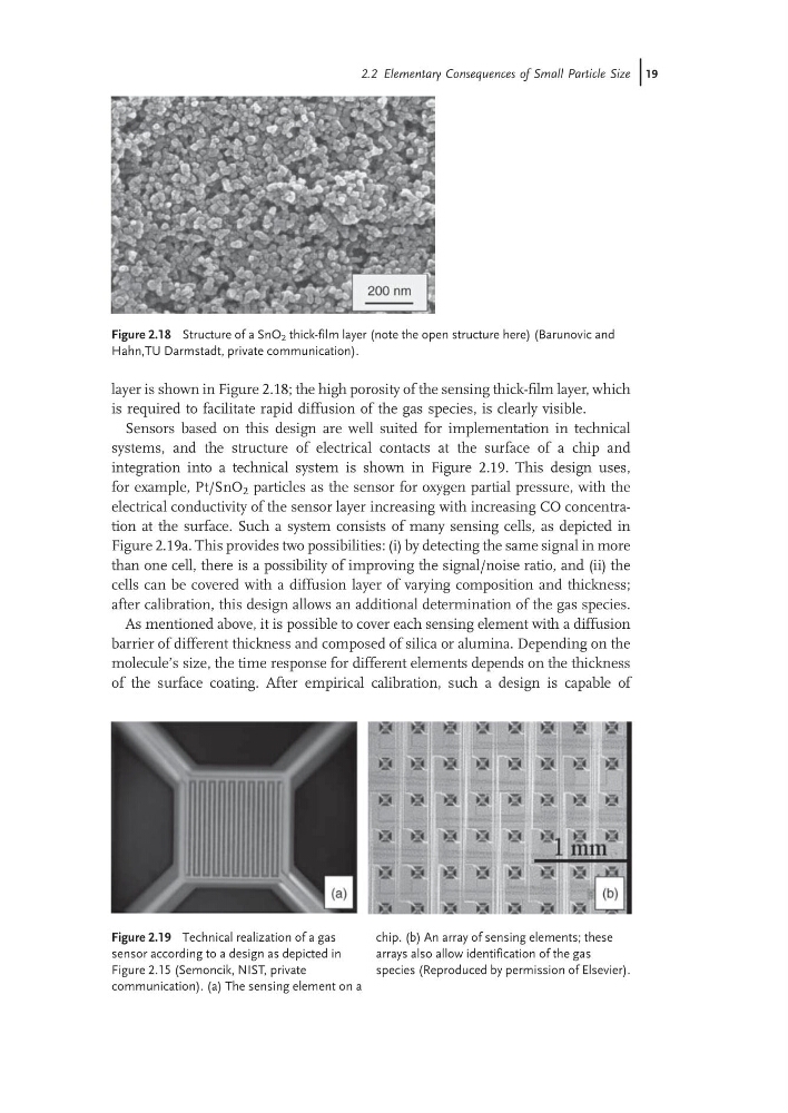
layer is shown in Figure 2.18; the high porosity of the sensing thick-film layer, which
is required to facilitate rapid diffusion of the gas species, is clearly visible.
Sensors based on this design are well suited for implementation in technical
systems, and the structure of electrical contacts at the surface of a chip and
integration into a technical system is shown in Figure 2.19. This design uses,
for example, Pt/SnO 2 particles as the sensor for oxygen partial pressure, with the
electrical conductivity of the sensor layer increasing with increasing CO concentration at the surface. Such a system consists of many sensing cells, as depicted in
Figure 2.19a. This provides two possibilities: (i) by detecting the same signal in more
than one cell, there is a possibility of improving the signal/noise ratio, and (ii) the
cells can be covered with a diffusion layer of varying composition and thickness;
after calibration, this design allows an additional determination of the gas species.
As mentioned above, it is possible to cover each sensing element with a diffusion
barrier of different thickness and composed of silica or alumina. Depending on the
molecule’s size, the time response for different elements depends on the thickness
of the surface coating. After empirical calibration, such a design is capable of
Figure 2.18 Structure of a SnO 2 thick-film layer (note the open structure here) (Barunovic and
Hahn,TU Darmstadt, private communication).
Figure 2.19 Technical realization of a gas
sensor according to a design as depicted in
Figure 2.15 (Semoncik, NIST, private
communication). (a) The sensing element on a
chip. (b) An array of sensing elements; these
arrays also allow identification of the gas
species (Reproduced by permission of Elsevier).
2.2 Elementary Consequences of Small Particle Size j19
is required to facilitate rapid diffusion of the gas species, is clearly visible.
Sensors based on this design are well suited for implementation in technical
systems, and the structure of electrical contacts at the surface of a chip and
integration into a technical system is shown in Figure 2.19. This design uses,
for example, Pt/SnO 2 particles as the sensor for oxygen partial pressure, with the
electrical conductivity of the sensor layer increasing with increasing CO concentration at the surface. Such a system consists of many sensing cells, as depicted in
Figure 2.19a. This provides two possibilities: (i) by detecting the same signal in more
than one cell, there is a possibility of improving the signal/noise ratio, and (ii) the
cells can be covered with a diffusion layer of varying composition and thickness;
after calibration, this design allows an additional determination of the gas species.
As mentioned above, it is possible to cover each sensing element with a diffusion
barrier of different thickness and composed of silica or alumina. Depending on the
molecule’s size, the time response for different elements depends on the thickness
of the surface coating. After empirical calibration, such a design is capable of
Figure 2.18 Structure of a SnO 2 thick-film layer (note the open structure here) (Barunovic and
Hahn,TU Darmstadt, private communication).
Figure 2.19 Technical realization of a gas
sensor according to a design as depicted in
Figure 2.15 (Semoncik, NIST, private
communication). (a) The sensing element on a
chip. (b) An array of sensing elements; these
arrays also allow identification of the gas
species (Reproduced by permission of Elsevier).
2.2 Elementary Consequences of Small Particle Size j19