

510
Y. Yoshida
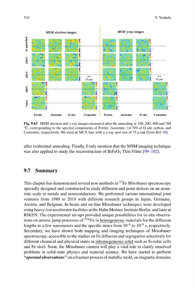
Fig. 9.63 MSM electron and γ-ray images measured after the annealing at 100, 200, 400 and 700
°C, corresponding to the spectral components of Ferrite, Austenite, 1st NN of O-site carbon, and
Cementite, respectively. We used an MCX lens with a γ-ray spot size of 75 μmφ [from Ref. 98]
after isothermal annealing. Finally, I only mention that the MSM imaging technique
was also applied to study the microstructure of BiFeO 3 Thin Films [99–102].
9.7 Summary
This chapter has demonstrated several new methods in
57 Fe Mössbauer spectroscopy
specially designed and constructed to study diffusion and point defects on an atomistic scale in metals and semiconductors. We performed various international joint
ventures from 1980 to 2019 with different research groups in Japan, Germany,
Austria, and Belgium. In-beam and on-line Mössbauer techniques were developed
using heavy-ion accelerator facilities at the Hahn Meitner Institute Berlin, and later at
RIKEN. The experimental set-ups provided unique possibilities for in-situ observations on atomic jump processes of
57m Fe in homogeneous materials for the diffusion
lengths to a few nanometers and the specific times from 10
–6 to 10
–8 s, respectively.
Secondary, we have shown both mapping and imaging techniques of Mössbauer
spectroscopy, accessible to the studies on Fe diffusion and segregation selectively for
different chemical and physical states in inhomogeneous solid such as Si-solar cells
and Fe steel. Soon, the Mössbauer camera will play a vital role to clarify unsolved
problems in solid-state physics and material science. We have started to perform
“operand observations” on a fracture process of metallic mold, on magnetic domains
Y. Yoshida
Fig. 9.63 MSM electron and γ-ray images measured after the annealing at 100, 200, 400 and 700
°C, corresponding to the spectral components of Ferrite, Austenite, 1st NN of O-site carbon, and
Cementite, respectively. We used an MCX lens with a γ-ray spot size of 75 μmφ [from Ref. 98]
after isothermal annealing. Finally, I only mention that the MSM imaging technique
was also applied to study the microstructure of BiFeO 3 Thin Films [99–102].
9.7 Summary
This chapter has demonstrated several new methods in
57 Fe Mössbauer spectroscopy
specially designed and constructed to study diffusion and point defects on an atomistic scale in metals and semiconductors. We performed various international joint
ventures from 1980 to 2019 with different research groups in Japan, Germany,
Austria, and Belgium. In-beam and on-line Mössbauer techniques were developed
using heavy-ion accelerator facilities at the Hahn Meitner Institute Berlin, and later at
RIKEN. The experimental set-ups provided unique possibilities for in-situ observations on atomic jump processes of
57m Fe in homogeneous materials for the diffusion
lengths to a few nanometers and the specific times from 10
–6 to 10
–8 s, respectively.
Secondary, we have shown both mapping and imaging techniques of Mössbauer
spectroscopy, accessible to the studies on Fe diffusion and segregation selectively for
different chemical and physical states in inhomogeneous solid such as Si-solar cells
and Fe steel. Soon, the Mössbauer camera will play a vital role to clarify unsolved
problems in solid-state physics and material science. We have started to perform
“operand observations” on a fracture process of metallic mold, on magnetic domains