

6.8 Practical Examples of Implementation …
629
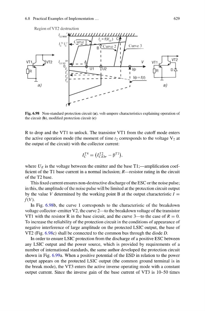
Fig. 6.98 Non-standard protection circuit (a), volt-ampere characteristics explaining operation of
the circuit (b), modified protection circuit (c)
R to drop and the VT1 to unlock. The transistor VT1 from the cutoff mode enters
the active operation mode (the moment of time t 2 corresponds to the voltage V 2 at
the output of the circuit) with the collector current:
I
T 4
C =
I
T 2
C Ebr − β
T 1
,
where U E is the voltage between the emitter and the base T1;—amplification coefficient of the T1 base current in a normal inclusion; R—resistor rating in the circuit
of the T2 base.
This fixed current ensures non-destructive discharge of the ESC or the noise pulse;
in this, the amplitude of the noise pulse will be limited at the protection circuit output
by the value V determined by the working point B at the output characteristic I =
f (V ).
In Fig. 6.98b, the curve 1 corresponds to the characteristic of the breakdown
voltage collector–emitter V2, the curve 2—to the breakdown voltage of the transistor
VT1 with the resistor R in the base circuit, and the curve 3—to the case of R = 0.
To increase the reliability of the protection circuit in the conditions of appearance of
negative interference of large amplitude on the protected LSIC output, the base of
VT2 (Fig. 6.98c) shall be connected to the common bus through the diode D.
In order to ensure LSIC protection from the discharge of a positive ESC between
any LSIC output and the power source, which is provided by requirements of a
number of international standards, the same author developed the protection circuit
shown in Fig. 6.99a. When a positive potential of the ESD in relation to the power
output appears on the protected LSIC output (the common ground terminal is in
the break mode), the VT3 enters the active inverse operating mode with a constant
output current. Since the inverse gain of the base current of VT3 is 10–50 times
629
Fig. 6.98 Non-standard protection circuit (a), volt-ampere characteristics explaining operation of
the circuit (b), modified protection circuit (c)
R to drop and the VT1 to unlock. The transistor VT1 from the cutoff mode enters
the active operation mode (the moment of time t 2 corresponds to the voltage V 2 at
the output of the circuit) with the collector current:
I
T 4
C =
I
T 2
C Ebr − β
T 1
,
where U E is the voltage between the emitter and the base T1;—amplification coefficient of the T1 base current in a normal inclusion; R—resistor rating in the circuit
of the T2 base.
This fixed current ensures non-destructive discharge of the ESC or the noise pulse;
in this, the amplitude of the noise pulse will be limited at the protection circuit output
by the value V determined by the working point B at the output characteristic I =
f (V ).
In Fig. 6.98b, the curve 1 corresponds to the characteristic of the breakdown
voltage collector–emitter V2, the curve 2—to the breakdown voltage of the transistor
VT1 with the resistor R in the base circuit, and the curve 3—to the case of R = 0.
To increase the reliability of the protection circuit in the conditions of appearance of
negative interference of large amplitude on the protected LSIC output, the base of
VT2 (Fig. 6.98c) shall be connected to the common bus through the diode D.
In order to ensure LSIC protection from the discharge of a positive ESC between
any LSIC output and the power source, which is provided by requirements of a
number of international standards, the same author developed the protection circuit
shown in Fig. 6.99a. When a positive potential of the ESD in relation to the power
output appears on the protected LSIC output (the common ground terminal is in
the break mode), the VT3 enters the active inverse operating mode with a constant
output current. Since the inverse gain of the base current of VT3 is 10–50 times