

6.8 Practical Examples of Implementation …
625
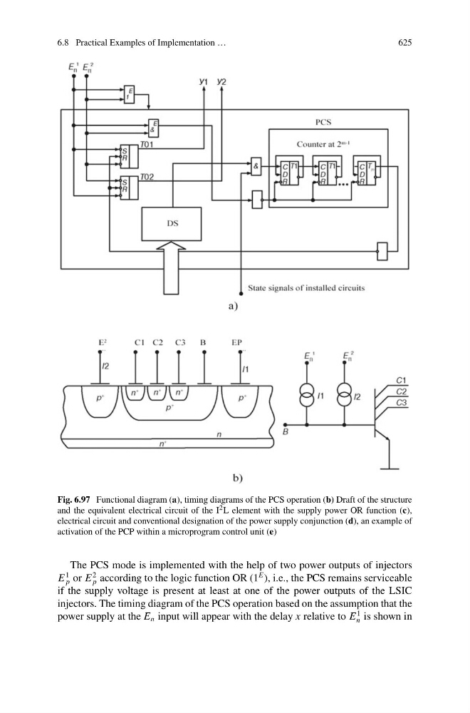
Fig. 6.97 Functional diagram (a), timing diagrams of the PCS operation (b) Draft of the structure
and the equivalent electrical circuit of the I 2 L element with the supply power OR function (c),
electrical circuit and conventional designation of the power supply conjunction (d), an example of
activation of the PCP within a microprogram control unit (e)
The PCS mode is implemented with the help of two power outputs of injectors
E
1
p or E
2
p according to the logic function OR (1
E ), i.e., the PCS remains serviceable
if the supply voltage is present at least at one of the power outputs of the LSIC
injectors. The timing diagram of the PCS operation based on the assumption that the
power supply at the E n input will appear with the delay x relative to E
1
n is shown in
625
Fig. 6.97 Functional diagram (a), timing diagrams of the PCS operation (b) Draft of the structure
and the equivalent electrical circuit of the I 2 L element with the supply power OR function (c),
electrical circuit and conventional designation of the power supply conjunction (d), an example of
activation of the PCP within a microprogram control unit (e)
The PCS mode is implemented with the help of two power outputs of injectors
E
1
p or E
2
p according to the logic function OR (1
E ), i.e., the PCS remains serviceable
if the supply voltage is present at least at one of the power outputs of the LSIC
injectors. The timing diagram of the PCS operation based on the assumption that the
power supply at the E n input will appear with the delay x relative to E
1
n is shown in