

592
6 Reverse Engineering of Microcircuits
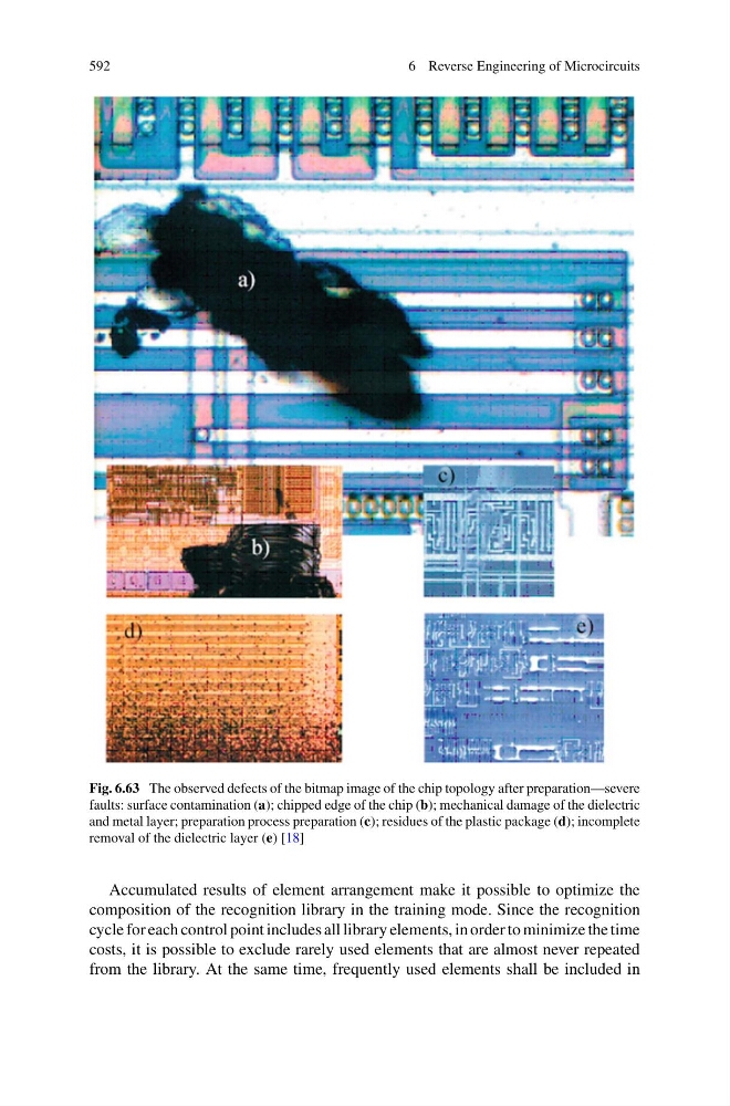
Fig. 6.63 The observed defects of the bitmap image of the chip topology after preparation—severe
faults: surface contamination (a); chipped edge of the chip (b); mechanical damage of the dielectric
and metal layer; preparation process preparation (c); residues of the plastic package (d); incomplete
removal of the dielectric layer (e) [18]
Accumulated results of element arrangement make it possible to optimize the
composition of the recognition library in the training mode. Since the recognition
cycle for each control point includes all library elements, in order to minimize the time
costs, it is possible to exclude rarely used elements that are almost never repeated
from the library. At the same time, frequently used elements shall be included in
6 Reverse Engineering of Microcircuits
Fig. 6.63 The observed defects of the bitmap image of the chip topology after preparation—severe
faults: surface contamination (a); chipped edge of the chip (b); mechanical damage of the dielectric
and metal layer; preparation process preparation (c); residues of the plastic package (d); incomplete
removal of the dielectric layer (e) [18]
Accumulated results of element arrangement make it possible to optimize the
composition of the recognition library in the training mode. Since the recognition
cycle for each control point includes all library elements, in order to minimize the time
costs, it is possible to exclude rarely used elements that are almost never repeated
from the library. At the same time, frequently used elements shall be included in