

6.3 Basics of Reverse-Engineering Art
543
6.3.2.9 An Example of Practical Implementation of Reverse
Engineering for ASIC
When used in an integrated fashion, all the above methods can be extremely powerful.
In order to illustrate it, let us consider a specific project implemented by Chipwork
[5]: this is a detailed study of a digital ASIC with built-in analog blocks and memory
blocks, which includes an embedded encrypted hardware part. The purpose of the
project was to ensure complete understanding of operation of this ASIC, build an
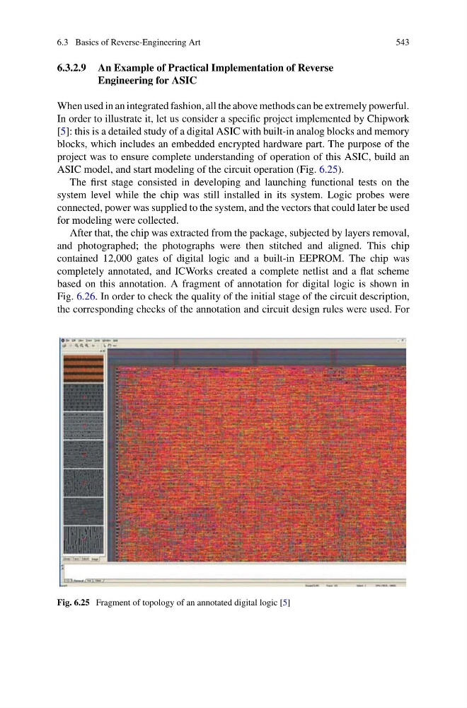
ASIC model, and start modeling of the circuit operation (Fig. 6.25).
The first stage consisted in developing and launching functional tests on the
system level while the chip was still installed in its system. Logic probes were
connected, power was supplied to the system, and the vectors that could later be used
for modeling were collected.
After that, the chip was extracted from the package, subjected by layers removal,
and photographed; the photographs were then stitched and aligned. This chip
contained 12,000 gates of digital logic and a built-in EEPROM. The chip was
completely annotated, and ICWorks created a complete netlist and a flat scheme
based on this annotation. A fragment of annotation for digital logic is shown in
Fig. 6.26. In order to check the quality of the initial stage of the circuit description,
the corresponding checks of the annotation and circuit design rules were used. For
Fig. 6.25 Fragment of topology of an annotated digital logic [5]
543
6.3.2.9 An Example of Practical Implementation of Reverse
Engineering for ASIC
When used in an integrated fashion, all the above methods can be extremely powerful.
In order to illustrate it, let us consider a specific project implemented by Chipwork
[5]: this is a detailed study of a digital ASIC with built-in analog blocks and memory
blocks, which includes an embedded encrypted hardware part. The purpose of the
project was to ensure complete understanding of operation of this ASIC, build an
ASIC model, and start modeling of the circuit operation (Fig. 6.25).
The first stage consisted in developing and launching functional tests on the
system level while the chip was still installed in its system. Logic probes were
connected, power was supplied to the system, and the vectors that could later be used
for modeling were collected.
After that, the chip was extracted from the package, subjected by layers removal,
and photographed; the photographs were then stitched and aligned. This chip
contained 12,000 gates of digital logic and a built-in EEPROM. The chip was
completely annotated, and ICWorks created a complete netlist and a flat scheme
based on this annotation. A fragment of annotation for digital logic is shown in
Fig. 6.26. In order to check the quality of the initial stage of the circuit description,
the corresponding checks of the annotation and circuit design rules were used. For
Fig. 6.25 Fragment of topology of an annotated digital logic [5]