

6.3 Basics of Reverse-Engineering Art
537
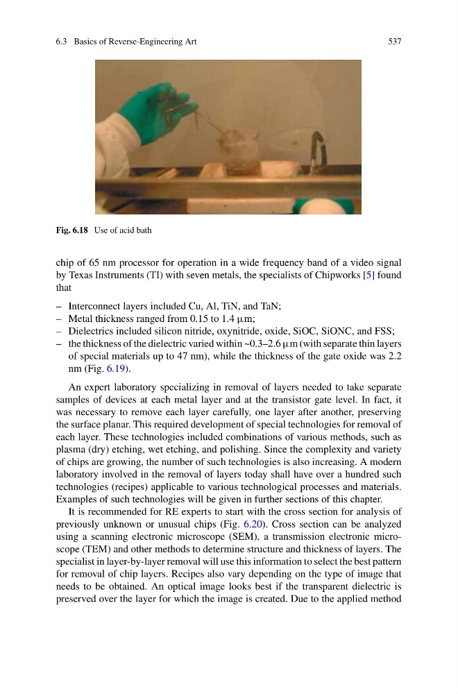
Fig. 6.18 Use of acid bath
chip of 65 nm processor for operation in a wide frequency band of a video signal
by Texas Instruments (TI) with seven metals, the specialists of Chipworks [5] found
that
– Interconnect layers included Cu, Al, TiN, and TaN;
– Metal thickness ranged from 0.15 to 1.4 μm;
– Dielectrics included silicon nitride, oxynitride, oxide, SiOC, SiONC, and FSS;
– the thickness of the dielectric varied within ~0.3–2.6 μm (with separate thin layers
of special materials up to 47 nm), while the thickness of the gate oxide was 2.2
nm (Fig. 6.19).
An expert laboratory specializing in removal of layers needed to take separate
samples of devices at each metal layer and at the transistor gate level. In fact, it
was necessary to remove each layer carefully, one layer after another, preserving
the surface planar. This required development of special technologies for removal of
each layer. These technologies included combinations of various methods, such as
plasma (dry) etching, wet etching, and polishing. Since the complexity and variety
of chips are growing, the number of such technologies is also increasing. A modern
laboratory involved in the removal of layers today shall have over a hundred such
technologies (recipes) applicable to various technological processes and materials.
Examples of such technologies will be given in further sections of this chapter.
It is recommended for RE experts to start with the cross section for analysis of
previously unknown or unusual chips (Fig. 6.20). Cross section can be analyzed
using a scanning electronic microscope (SEM), a transmission electronic microscope (TEM) and other methods to determine structure and thickness of layers. The
specialist in layer-by-layer removal will use this information to select the best pattern
for removal of chip layers. Recipes also vary depending on the type of image that
needs to be obtained. An optical image looks best if the transparent dielectric is
preserved over the layer for which the image is created. Due to the applied method
537
Fig. 6.18 Use of acid bath
chip of 65 nm processor for operation in a wide frequency band of a video signal
by Texas Instruments (TI) with seven metals, the specialists of Chipworks [5] found
that
– Interconnect layers included Cu, Al, TiN, and TaN;
– Metal thickness ranged from 0.15 to 1.4 μm;
– Dielectrics included silicon nitride, oxynitride, oxide, SiOC, SiONC, and FSS;
– the thickness of the dielectric varied within ~0.3–2.6 μm (with separate thin layers
of special materials up to 47 nm), while the thickness of the gate oxide was 2.2
nm (Fig. 6.19).
An expert laboratory specializing in removal of layers needed to take separate
samples of devices at each metal layer and at the transistor gate level. In fact, it
was necessary to remove each layer carefully, one layer after another, preserving
the surface planar. This required development of special technologies for removal of
each layer. These technologies included combinations of various methods, such as
plasma (dry) etching, wet etching, and polishing. Since the complexity and variety
of chips are growing, the number of such technologies is also increasing. A modern
laboratory involved in the removal of layers today shall have over a hundred such
technologies (recipes) applicable to various technological processes and materials.
Examples of such technologies will be given in further sections of this chapter.
It is recommended for RE experts to start with the cross section for analysis of
previously unknown or unusual chips (Fig. 6.20). Cross section can be analyzed
using a scanning electronic microscope (SEM), a transmission electronic microscope (TEM) and other methods to determine structure and thickness of layers. The
specialist in layer-by-layer removal will use this information to select the best pattern
for removal of chip layers. Recipes also vary depending on the type of image that
needs to be obtained. An optical image looks best if the transparent dielectric is
preserved over the layer for which the image is created. Due to the applied method