

516
6 Reverse Engineering of Microcircuits
formed commissions and inspections for comparative analysis of the products of the
legal owner of potentially malicious competitors (reproduced).
Of course, development of reverse-engineering methods shall take into account
modern technological innovations, as new organic and inorganic materials appear,
as well as new so-called k-dielectrics, new types and designs of optical waveguides,
new types and materials of solar batteries, which is a fairly difficult task due to
extremely low concentrations of used impurities and an extremely wide range of
possible combinations of applied semiconductor materials (silicon, silicon carbide,
helium arsenide, etc.).
Now, surfaces of semiconductor circuit chip contain millions of various transistors; new microcircuit architectures and algorithms of their operation emerge,
and various types of their interface are developed actively; modern qualified reverseengineering specialists shall account for all these factors and use them in their difficult
work.
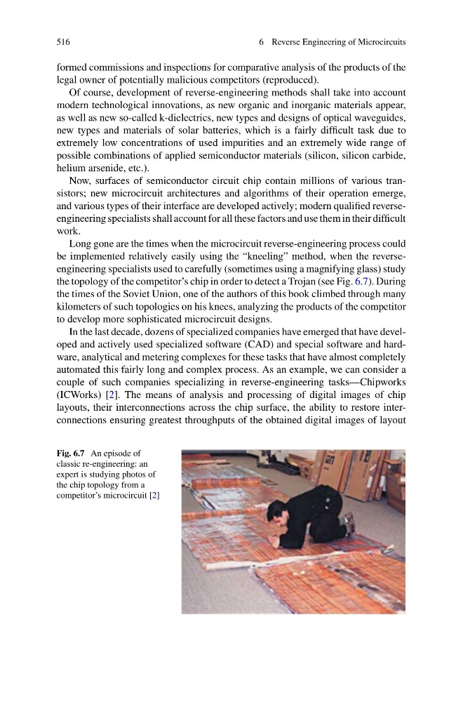
Long gone are the times when the microcircuit reverse-engineering process could
be implemented relatively easily using the “kneeling” method, when the reverseengineering specialists used to carefully (sometimes using a magnifying glass) study
the topology of the competitor’s chip in order to detect a Trojan (see Fig. 6.7). During
the times of the Soviet Union, one of the authors of this book climbed through many
kilometers of such topologies on his knees, analyzing the products of the competitor
to develop more sophisticated microcircuit designs.
In the last decade, dozens of specialized companies have emerged that have developed and actively used specialized software (CAD) and special software and hardware, analytical and metering complexes for these tasks that have almost completely
automated this fairly long and complex process. As an example, we can consider a
couple of such companies specializing in reverse-engineering tasks—Chipworks
(ICWorks) [2]. The means of analysis and processing of digital images of chip
layouts, their interconnections across the chip surface, the ability to restore interconnections ensuring greatest throughputs of the obtained digital images of layout
Fig. 6.7 An episode of
classic re-engineering: an
expert is studying photos of
the chip topology from a
competitor’s microcircuit [2]
6 Reverse Engineering of Microcircuits
formed commissions and inspections for comparative analysis of the products of the
legal owner of potentially malicious competitors (reproduced).
Of course, development of reverse-engineering methods shall take into account
modern technological innovations, as new organic and inorganic materials appear,
as well as new so-called k-dielectrics, new types and designs of optical waveguides,
new types and materials of solar batteries, which is a fairly difficult task due to
extremely low concentrations of used impurities and an extremely wide range of
possible combinations of applied semiconductor materials (silicon, silicon carbide,
helium arsenide, etc.).
Now, surfaces of semiconductor circuit chip contain millions of various transistors; new microcircuit architectures and algorithms of their operation emerge,
and various types of their interface are developed actively; modern qualified reverseengineering specialists shall account for all these factors and use them in their difficult
work.
Long gone are the times when the microcircuit reverse-engineering process could
be implemented relatively easily using the “kneeling” method, when the reverseengineering specialists used to carefully (sometimes using a magnifying glass) study
the topology of the competitor’s chip in order to detect a Trojan (see Fig. 6.7). During
the times of the Soviet Union, one of the authors of this book climbed through many
kilometers of such topologies on his knees, analyzing the products of the competitor
to develop more sophisticated microcircuit designs.
In the last decade, dozens of specialized companies have emerged that have developed and actively used specialized software (CAD) and special software and hardware, analytical and metering complexes for these tasks that have almost completely
automated this fairly long and complex process. As an example, we can consider a
couple of such companies specializing in reverse-engineering tasks—Chipworks
(ICWorks) [2]. The means of analysis and processing of digital images of chip
layouts, their interconnections across the chip surface, the ability to restore interconnections ensuring greatest throughputs of the obtained digital images of layout
Fig. 6.7 An episode of
classic re-engineering: an
expert is studying photos of
the chip topology from a
competitor’s microcircuit [2]