

1 Introduction to Laser Micro-to-Nano Manufacturing
61
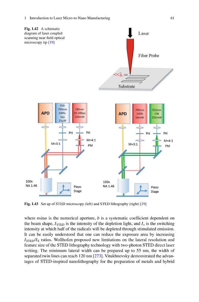
Fig. 1.42 A schematic
diagram of laser coupled
scanning near field optical
microscopy tip [19]
Fig. 1.43 Set up of STED microscopy (left) and STED lithography (right) [19]
where nsinα is the numerical aperture, b is a systematic coefficient dependent on
the beam shape, I STED is the intensity of the depletion light, and I s is the switching
intensity at which half of the radicals will be depleted through stimulated emission.
It can be easily understood that one can reduce the exposure area by increasing
I STED /I S ratios. Wollhofen proposed new limitations on the lateral resolution and
feature size of the STED lithography technology with two-photon STED direct laser
writing. The minimum lateral width can be prepared up to 55 nm, the width of
separated twin lines can reach 120 nm [273]. Vitukhnovsky demonstrated the advantages of STED-inspired nanolithography for the preparation of metals and hybrid
61
Fig. 1.42 A schematic
diagram of laser coupled
scanning near field optical
microscopy tip [19]
Fig. 1.43 Set up of STED microscopy (left) and STED lithography (right) [19]
where nsinα is the numerical aperture, b is a systematic coefficient dependent on
the beam shape, I STED is the intensity of the depletion light, and I s is the switching
intensity at which half of the radicals will be depleted through stimulated emission.
It can be easily understood that one can reduce the exposure area by increasing
I STED /I S ratios. Wollhofen proposed new limitations on the lateral resolution and
feature size of the STED lithography technology with two-photon STED direct laser
writing. The minimum lateral width can be prepared up to 55 nm, the width of
separated twin lines can reach 120 nm [273]. Vitukhnovsky demonstrated the advantages of STED-inspired nanolithography for the preparation of metals and hybrid