

52
A. Hu et al.
Table 1.3 shows a comparison between conventional joining techniques and nanojoining innovations [41]. Solid-state diffusion driven by surface energy has enabled
welding of two bare Au nanowires in vacuum at room temperature [47] and joining
of two silver nanowires after removal of the surface-capping amorphous layer at an
ambient atmosphere [48]. However, this solid-state diffusion is difficult to achieve
joining with an arbitrary angle unless applying the external excitation energy, such
as a head-to-side joining (T-shape) since the capping layer on the sidewall is thicker
than the layer at the wire head [48]. Although the Joule heating was proposed to
join metallic nanowires in case of contact wires [182, 183], the so-called nanoscopic
resistance spot welding can be only applied to conductive nanowires. A mechanical
pressing with nanoindentation was also developed to join nanowires to the substrate
[178, 179]. Unfortunately, this press will significantly deform the wire head. On the
other hand, the substrate can be also deformed seriously by Joule heating, mechanical pressure and thermal annealing unless the processing parameters, e.g., current,
pressure, and temperature, are accurately controlled. Compared with these joining
methods, photonic sintering was conducted for joining metal nanowires at arbitrary
contact angles, which enables non-contact processing and good thermal management
to minimize the damage of the substrate and nanomaterials. Due to self-localized
plasmonic excitation [94], this plasmonic heat can lead to the perfect joining of adjacent and/or contact nanowires. A continuous-wave laser was reported to braze the
crossed NWs [196], which is similar to autogenous laser brazing for metal microjoining [203]. However, laser joined metal NWs display a polycrystalline nature with
lots of defects at the joined regions [88, 197, 204]. This is quite different from a selforiented joining with solid-state diffusion where a clear lattice matching is founded.
Femtosecond laser joining and a laser-healing of cutting wires has shown possible
epitaxial recrystallization or enhanced grain orientation [88, 204, 205]. Therefore,
precise control of laser parameters based on the understanding of the interaction of
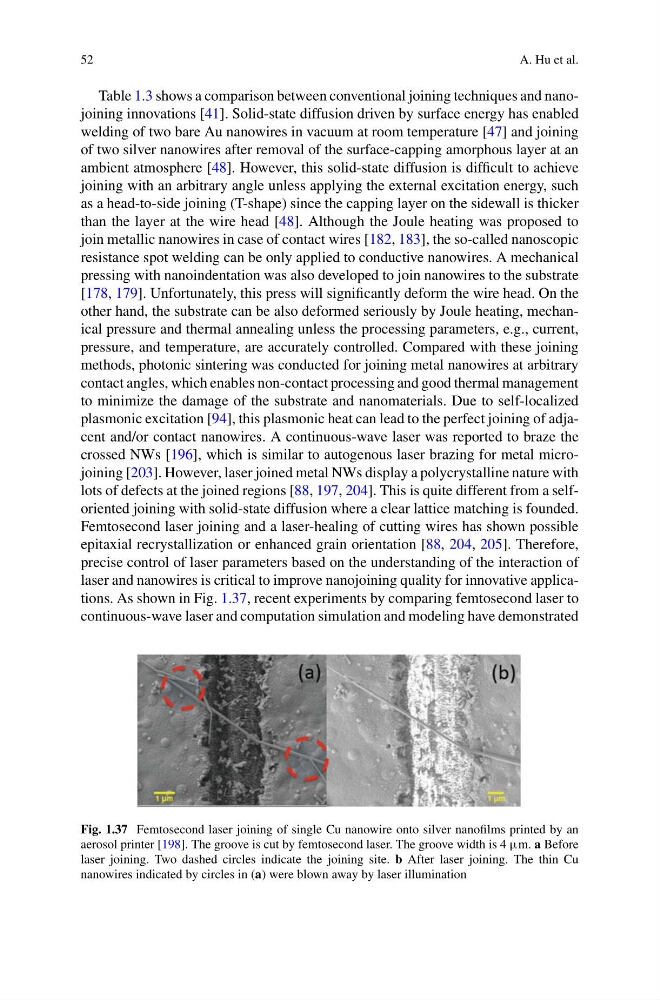
laser and nanowires is critical to improve nanojoining quality for innovative applications. As shown in Fig. 1.37, recent experiments by comparing femtosecond laser to
continuous-wave laser and computation simulation and modeling have demonstrated
Fig. 1.37 Femtosecond laser joining of single Cu nanowire onto silver nanofilms printed by an
aerosol printer [198]. The groove is cut by femtosecond laser. The groove width is 4 μm. a Before
laser joining. Two dashed circles indicate the joining site. b After laser joining. The thin Cu
nanowires indicated by circles in (a) were blown away by laser illumination
A. Hu et al.
Table 1.3 shows a comparison between conventional joining techniques and nanojoining innovations [41]. Solid-state diffusion driven by surface energy has enabled
welding of two bare Au nanowires in vacuum at room temperature [47] and joining
of two silver nanowires after removal of the surface-capping amorphous layer at an
ambient atmosphere [48]. However, this solid-state diffusion is difficult to achieve
joining with an arbitrary angle unless applying the external excitation energy, such
as a head-to-side joining (T-shape) since the capping layer on the sidewall is thicker
than the layer at the wire head [48]. Although the Joule heating was proposed to
join metallic nanowires in case of contact wires [182, 183], the so-called nanoscopic
resistance spot welding can be only applied to conductive nanowires. A mechanical
pressing with nanoindentation was also developed to join nanowires to the substrate
[178, 179]. Unfortunately, this press will significantly deform the wire head. On the
other hand, the substrate can be also deformed seriously by Joule heating, mechanical pressure and thermal annealing unless the processing parameters, e.g., current,
pressure, and temperature, are accurately controlled. Compared with these joining
methods, photonic sintering was conducted for joining metal nanowires at arbitrary
contact angles, which enables non-contact processing and good thermal management
to minimize the damage of the substrate and nanomaterials. Due to self-localized
plasmonic excitation [94], this plasmonic heat can lead to the perfect joining of adjacent and/or contact nanowires. A continuous-wave laser was reported to braze the
crossed NWs [196], which is similar to autogenous laser brazing for metal microjoining [203]. However, laser joined metal NWs display a polycrystalline nature with
lots of defects at the joined regions [88, 197, 204]. This is quite different from a selforiented joining with solid-state diffusion where a clear lattice matching is founded.
Femtosecond laser joining and a laser-healing of cutting wires has shown possible
epitaxial recrystallization or enhanced grain orientation [88, 204, 205]. Therefore,
precise control of laser parameters based on the understanding of the interaction of
laser and nanowires is critical to improve nanojoining quality for innovative applications. As shown in Fig. 1.37, recent experiments by comparing femtosecond laser to
continuous-wave laser and computation simulation and modeling have demonstrated
Fig. 1.37 Femtosecond laser joining of single Cu nanowire onto silver nanofilms printed by an
aerosol printer [198]. The groove is cut by femtosecond laser. The groove width is 4 μm. a Before
laser joining. Two dashed circles indicate the joining site. b After laser joining. The thin Cu
nanowires indicated by circles in (a) were blown away by laser illumination