

1 Introduction to Laser Micro-to-Nano Manufacturing
35
beam diameter and 120 kHz of pulse repetition rate. Heat flow from electron to the
lattice, Q el→latt is calculated using the electron-lattice coupling coefficient (g, W/m
3
K) from the literature [124] and the difference between T e and T l , i.e., Q el→latt =
gV (T e – T l ). Conduction heat flow and stored thermal energy change for electron
and lattice [Q el,cond and E el in (2) and Q latt,cond and E latt in (3)] are calculated using
the electron thermal conductivity, k e = 385 W/m K, lattice thermal conductivity, k l
= 17 W/m K, [125] temperature-dependent electron volumetric heat capacity C e
(J/m
3 K) from [124] and lattice volumetric heat capacity, C l = 3.45 × 10
6 J/m
3 K for
Cu [125]. Convection and radiation (Q conv and Q rad ) are included in the T l analysis
only and calculated as the single-temperature modeling using the same properties.
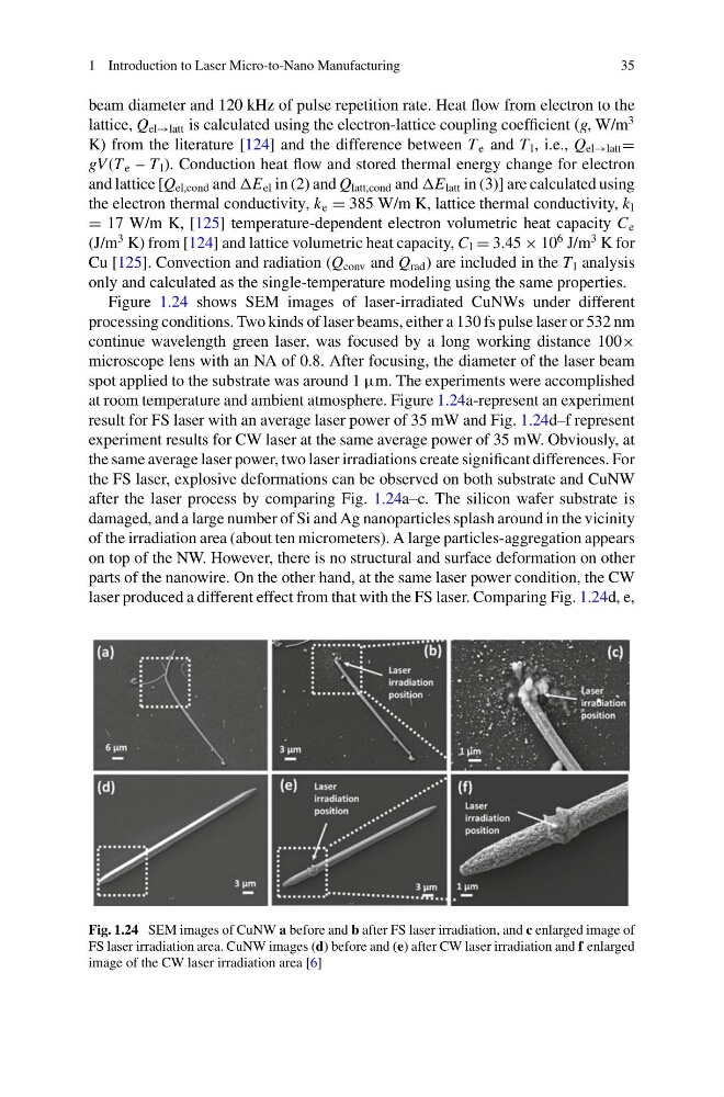
Figure 1.24 shows SEM images of laser-irradiated CuNWs under different
processing conditions. Two kinds of laser beams, either a 130 fs pulse laser or 532 nm
continue wavelength green laser, was focused by a long working distance 100×
microscope lens with an NA of 0.8. After focusing, the diameter of the laser beam
spot applied to the substrate was around 1 μm. The experiments were accomplished
at room temperature and ambient atmosphere. Figure 1.24a-represent an experiment
result for FS laser with an average laser power of 35 mW and Fig. 1.24d–f represent
experiment results for CW laser at the same average power of 35 mW. Obviously, at
the same average laser power, two laser irradiations create significant differences. For
the FS laser, explosive deformations can be observed on both substrate and CuNW
after the laser process by comparing Fig. 1.24a–c. The silicon wafer substrate is
damaged, and a large number of Si and Ag nanoparticles splash around in the vicinity
of the irradiation area (about ten micrometers). A large particles-aggregation appears
on top of the NW. However, there is no structural and surface deformation on other
parts of the nanowire. On the other hand, at the same laser power condition, the CW
laser produced a different effect from that with the FS laser. Comparing Fig. 1.24d, e,
Fig. 1.24 SEM images of CuNW a before and b after FS laser irradiation, and c enlarged image of
FS laser irradiation area. CuNW images (d) before and (e) after CW laser irradiation and f enlarged
image of the CW laser irradiation area [6]
35
beam diameter and 120 kHz of pulse repetition rate. Heat flow from electron to the
lattice, Q el→latt is calculated using the electron-lattice coupling coefficient (g, W/m
3
K) from the literature [124] and the difference between T e and T l , i.e., Q el→latt =
gV (T e – T l ). Conduction heat flow and stored thermal energy change for electron
and lattice [Q el,cond and E el in (2) and Q latt,cond and E latt in (3)] are calculated using
the electron thermal conductivity, k e = 385 W/m K, lattice thermal conductivity, k l
= 17 W/m K, [125] temperature-dependent electron volumetric heat capacity C e
(J/m
3 K) from [124] and lattice volumetric heat capacity, C l = 3.45 × 10
6 J/m
3 K for
Cu [125]. Convection and radiation (Q conv and Q rad ) are included in the T l analysis
only and calculated as the single-temperature modeling using the same properties.
Figure 1.24 shows SEM images of laser-irradiated CuNWs under different
processing conditions. Two kinds of laser beams, either a 130 fs pulse laser or 532 nm
continue wavelength green laser, was focused by a long working distance 100×
microscope lens with an NA of 0.8. After focusing, the diameter of the laser beam
spot applied to the substrate was around 1 μm. The experiments were accomplished
at room temperature and ambient atmosphere. Figure 1.24a-represent an experiment
result for FS laser with an average laser power of 35 mW and Fig. 1.24d–f represent
experiment results for CW laser at the same average power of 35 mW. Obviously, at
the same average laser power, two laser irradiations create significant differences. For
the FS laser, explosive deformations can be observed on both substrate and CuNW
after the laser process by comparing Fig. 1.24a–c. The silicon wafer substrate is
damaged, and a large number of Si and Ag nanoparticles splash around in the vicinity
of the irradiation area (about ten micrometers). A large particles-aggregation appears
on top of the NW. However, there is no structural and surface deformation on other
parts of the nanowire. On the other hand, at the same laser power condition, the CW
laser produced a different effect from that with the FS laser. Comparing Fig. 1.24d, e,
Fig. 1.24 SEM images of CuNW a before and b after FS laser irradiation, and c enlarged image of
FS laser irradiation area. CuNW images (d) before and (e) after CW laser irradiation and f enlarged
image of the CW laser irradiation area [6]