

10 Laser Scanning Stereolithography
309
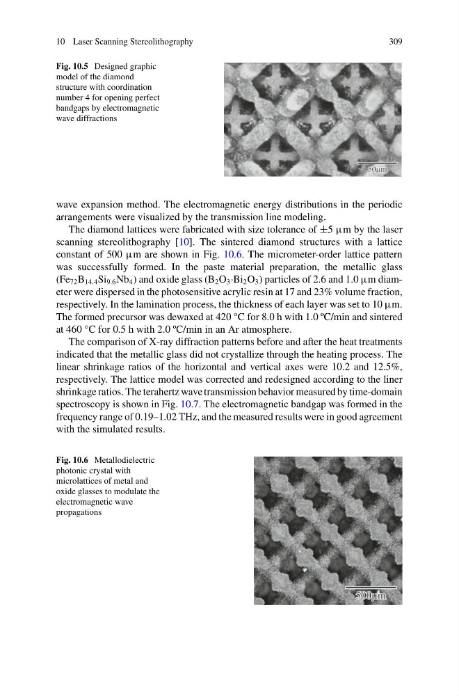
Fig. 10.5 Designed graphic
model of the diamond
structure with coordination
number 4 for opening perfect
bandgaps by electromagnetic
wave diffractions
wave expansion method. The electromagnetic energy distributions in the periodic
arrangements were visualized by the transmission line modeling.
The diamond lattices were fabricated with size tolerance of ±5 µm by the laser
scanning stereolithography [10]. The sintered diamond structures with a lattice
constant of 500 µm are shown in Fig. 10.6. The micrometer-order lattice pattern
was successfully formed. In the paste material preparation, the metallic glass
(Fe 72 B 14.4 Si 9.6 Nb 4 ) and oxide glass (B 2 O 3 ·Bi 2 O 3 ) particles of 2.6 and 1.0 µm diameter were dispersed in the photosensitive acrylic resin at 17 and 23% volume fraction,
respectively. In the lamination process, the thickness of each layer was set to 10 µm.
The formed precursor was dewaxed at 420 °C for 8.0 h with 1.0 ºC/min and sintered
at 460 °C for 0.5 h with 2.0 ºC/min in an Ar atmosphere.
The comparison of X-ray diffraction patterns before and after the heat treatments
indicated that the metallic glass did not crystallize through the heating process. The
linear shrinkage ratios of the horizontal and vertical axes were 10.2 and 12.5%,
respectively. The lattice model was corrected and redesigned according to the liner
shrinkage ratios. The terahertz wave transmission behavior measured by time-domain
spectroscopy is shown in Fig. 10.7. The electromagnetic bandgap was formed in the
frequency range of 0.19–1.02 THz, and the measured results were in good agreement
with the simulated results.
Fig. 10.6 Metallodielectric
photonic crystal with
microlattices of metal and
oxide glasses to modulate the
electromagnetic wave
propagations
309
Fig. 10.5 Designed graphic
model of the diamond
structure with coordination
number 4 for opening perfect
bandgaps by electromagnetic
wave diffractions
wave expansion method. The electromagnetic energy distributions in the periodic
arrangements were visualized by the transmission line modeling.
The diamond lattices were fabricated with size tolerance of ±5 µm by the laser
scanning stereolithography [10]. The sintered diamond structures with a lattice
constant of 500 µm are shown in Fig. 10.6. The micrometer-order lattice pattern
was successfully formed. In the paste material preparation, the metallic glass
(Fe 72 B 14.4 Si 9.6 Nb 4 ) and oxide glass (B 2 O 3 ·Bi 2 O 3 ) particles of 2.6 and 1.0 µm diameter were dispersed in the photosensitive acrylic resin at 17 and 23% volume fraction,
respectively. In the lamination process, the thickness of each layer was set to 10 µm.
The formed precursor was dewaxed at 420 °C for 8.0 h with 1.0 ºC/min and sintered
at 460 °C for 0.5 h with 2.0 ºC/min in an Ar atmosphere.
The comparison of X-ray diffraction patterns before and after the heat treatments
indicated that the metallic glass did not crystallize through the heating process. The
linear shrinkage ratios of the horizontal and vertical axes were 10.2 and 12.5%,
respectively. The lattice model was corrected and redesigned according to the liner
shrinkage ratios. The terahertz wave transmission behavior measured by time-domain
spectroscopy is shown in Fig. 10.7. The electromagnetic bandgap was formed in the
frequency range of 0.19–1.02 THz, and the measured results were in good agreement
with the simulated results.
Fig. 10.6 Metallodielectric
photonic crystal with
microlattices of metal and
oxide glasses to modulate the
electromagnetic wave
propagations