

10
A. Hu et al.
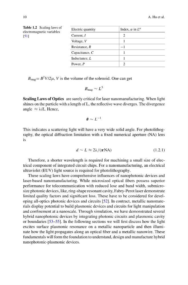
Table 1.2 Scaling laws of
electromagnetic variables
[51]
Electric quantity
Index, α in L α
Current, I
2
Voltage, V
1
Resistance, R
−1
Capacitance, C
1
Inductance, L
1
Power, P
2
B mag = B
2 V /2μ, V is the volume of the solenoid. One can get
B mag ∼ L
5
Scaling Laws of Optics are surely critical for laser nanomanufacturing. When light
shines on the particle with a length of L, the reflective wave diverges. The divergence
angle ≈ λ/L. Hence,
θ ∼ L
−1
This indicates a scattering light will have a very wide solid angle. For photolithography, the optical diffraction limitation with a fixed numerical aperture (NA) lens
is
d ∼ L ≈ 2λ/(πNA)
(1.2.1)
Therefore, a shorter wavelength is required for machining a small size of electrical component of integrated circuit chips. For a nanomanufacturing, an electrical
ultraviolet (EUV) light source is required for photolithography.
These scaling laws have comprehensive influences of nanophotonic devices and
laser-based nanomanufacturing. While microsized optical fibers possess superior
performance for telecommunication with reduced lose and band width, submicrosize photonic devices, like, ring-shape resonant cavity, Fabry-Perot laser demonstrate
limited quality factors and significant loss. These have to be considered for developing all-optics photonic devices and circuits [52]. In contract, metallic nanomaterials display potential to build plasmonic devices and circuits for light manipulation
and confinement at a nanoscale. Through simulation, we have demonstrated several
hybrid nanophotonic devices by integrating photonic circuits and plasmonic cavity
or boundaries [53–55]. In the following sections we will first discuss how the light
excites surface plasmonic resonance on a metallic nanoparticle and then illuminate how the light propagates along an optical fiber and a metallic nanowire. These
fundamentals will form the foundation to understand, design and manufacture hybrid
nanophotonic-plasmonic devices.
A. Hu et al.
Table 1.2 Scaling laws of
electromagnetic variables
[51]
Electric quantity
Index, α in L α
Current, I
2
Voltage, V
1
Resistance, R
−1
Capacitance, C
1
Inductance, L
1
Power, P
2
B mag = B
2 V /2μ, V is the volume of the solenoid. One can get
B mag ∼ L
5
Scaling Laws of Optics are surely critical for laser nanomanufacturing. When light
shines on the particle with a length of L, the reflective wave diverges. The divergence
angle ≈ λ/L. Hence,
θ ∼ L
−1
This indicates a scattering light will have a very wide solid angle. For photolithography, the optical diffraction limitation with a fixed numerical aperture (NA) lens
is
d ∼ L ≈ 2λ/(πNA)
(1.2.1)
Therefore, a shorter wavelength is required for machining a small size of electrical component of integrated circuit chips. For a nanomanufacturing, an electrical
ultraviolet (EUV) light source is required for photolithography.
These scaling laws have comprehensive influences of nanophotonic devices and
laser-based nanomanufacturing. While microsized optical fibers possess superior
performance for telecommunication with reduced lose and band width, submicrosize photonic devices, like, ring-shape resonant cavity, Fabry-Perot laser demonstrate
limited quality factors and significant loss. These have to be considered for developing all-optics photonic devices and circuits [52]. In contract, metallic nanomaterials display potential to build plasmonic devices and circuits for light manipulation
and confinement at a nanoscale. Through simulation, we have demonstrated several
hybrid nanophotonic devices by integrating photonic circuits and plasmonic cavity
or boundaries [53–55]. In the following sections we will first discuss how the light
excites surface plasmonic resonance on a metallic nanoparticle and then illuminate how the light propagates along an optical fiber and a metallic nanowire. These
fundamentals will form the foundation to understand, design and manufacture hybrid
nanophotonic-plasmonic devices.