

206
F. Chen and J. R. V. de Aldana
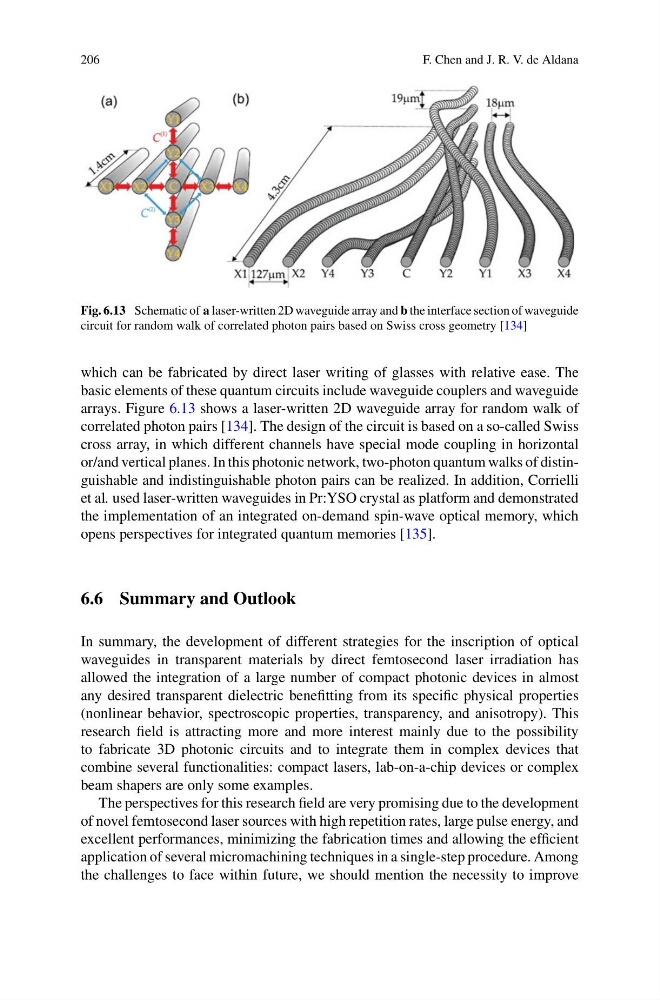
Fig. 6.13 Schematic of a laser-written 2D waveguide array and b the interface section of waveguide
circuit for random walk of correlated photon pairs based on Swiss cross geometry [134]
which can be fabricated by direct laser writing of glasses with relative ease. The
basic elements of these quantum circuits include waveguide couplers and waveguide
arrays. Figure 6.13 shows a laser-written 2D waveguide array for random walk of
correlated photon pairs [134]. The design of the circuit is based on a so-called Swiss
cross array, in which different channels have special mode coupling in horizontal
or/and vertical planes. In this photonic network, two-photon quantum walks of distinguishable and indistinguishable photon pairs can be realized. In addition, Corrielli
et al. used laser-written waveguides in Pr:YSO crystal as platform and demonstrated
the implementation of an integrated on-demand spin-wave optical memory, which
opens perspectives for integrated quantum memories [135].
6.6 Summary and Outlook
In summary, the development of different strategies for the inscription of optical
waveguides in transparent materials by direct femtosecond laser irradiation has
allowed the integration of a large number of compact photonic devices in almost
any desired transparent dielectric benefitting from its specific physical properties
(nonlinear behavior, spectroscopic properties, transparency, and anisotropy). This
research field is attracting more and more interest mainly due to the possibility
to fabricate 3D photonic circuits and to integrate them in complex devices that
combine several functionalities: compact lasers, lab-on-a-chip devices or complex
beam shapers are only some examples.
The perspectives for this research field are very promising due to the development
of novel femtosecond laser sources with high repetition rates, large pulse energy, and
excellent performances, minimizing the fabrication times and allowing the efficient
application of several micromachining techniques in a single-step procedure. Among
the challenges to face within future, we should mention the necessity to improve
F. Chen and J. R. V. de Aldana
Fig. 6.13 Schematic of a laser-written 2D waveguide array and b the interface section of waveguide
circuit for random walk of correlated photon pairs based on Swiss cross geometry [134]
which can be fabricated by direct laser writing of glasses with relative ease. The
basic elements of these quantum circuits include waveguide couplers and waveguide
arrays. Figure 6.13 shows a laser-written 2D waveguide array for random walk of
correlated photon pairs [134]. The design of the circuit is based on a so-called Swiss
cross array, in which different channels have special mode coupling in horizontal
or/and vertical planes. In this photonic network, two-photon quantum walks of distinguishable and indistinguishable photon pairs can be realized. In addition, Corrielli
et al. used laser-written waveguides in Pr:YSO crystal as platform and demonstrated
the implementation of an integrated on-demand spin-wave optical memory, which
opens perspectives for integrated quantum memories [135].
6.6 Summary and Outlook
In summary, the development of different strategies for the inscription of optical
waveguides in transparent materials by direct femtosecond laser irradiation has
allowed the integration of a large number of compact photonic devices in almost
any desired transparent dielectric benefitting from its specific physical properties
(nonlinear behavior, spectroscopic properties, transparency, and anisotropy). This
research field is attracting more and more interest mainly due to the possibility
to fabricate 3D photonic circuits and to integrate them in complex devices that
combine several functionalities: compact lasers, lab-on-a-chip devices or complex
beam shapers are only some examples.
The perspectives for this research field are very promising due to the development
of novel femtosecond laser sources with high repetition rates, large pulse energy, and
excellent performances, minimizing the fabrication times and allowing the efficient
application of several micromachining techniques in a single-step procedure. Among
the challenges to face within future, we should mention the necessity to improve