

198
F. Chen and J. R. V. de Aldana
chips [9, 114, 115]. Moreover, due to the possibility to control the optical properties of the waveguides by the multi-scan technique, the 3D photonic circuits can be
designed to operate even in the mid-infrared [116].
Most of these devices have been implemented in glass substrates (Sect. 6.4.1)
due to the relative simplicity of the fabrication procedure in such targets. However,
there is much interest in the integration of such structures in dielectric crystals [6]
due to their impressive optical properties, as high transparency range, or nonlinear
coefficients. Several research groups have been working towards the fabrication of
complex photonic devices in crystals using femtosecond laser direct inscription, but
most of the research work has been restricted to planar structures based on simple
waveguides. This is due to the large complexity of the problem: On the one hand,
Type-I modification typically produces a refractive index decrease (instead of an
increase) in most of the crystals and, on the other hand, anisotropy in crystalline
materials makes the fabrication highly sensitive to irradiation conditions [117]. In
crystals in which a refractive index increase can be produced by Type-I modification,
such as LiNbO 3 , Bi 4 Ge 3 O 12 , or YCa 4 O(BO 3 ) 3 , 3D devices such as waveguide arrays
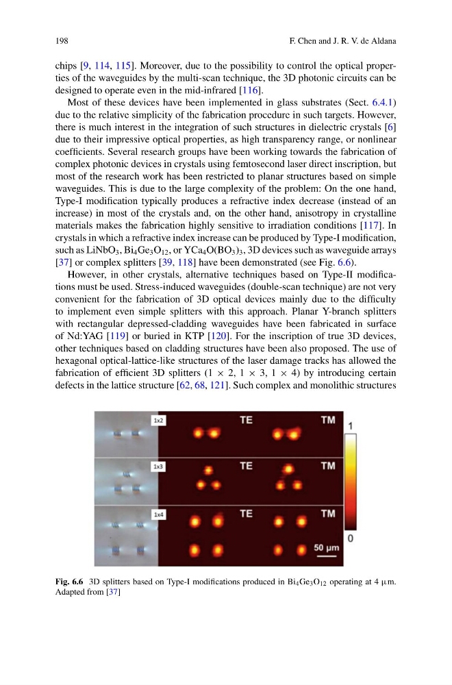
[37] or complex splitters [39, 118] have been demonstrated (see Fig. 6.6).
However, in other crystals, alternative techniques based on Type-II modifications must be used. Stress-induced waveguides (double-scan technique) are not very
convenient for the fabrication of 3D optical devices mainly due to the difficulty
to implement even simple splitters with this approach. Planar Y-branch splitters
with rectangular depressed-cladding waveguides have been fabricated in surface
of Nd:YAG [119] or buried in KTP [120]. For the inscription of true 3D devices,
other techniques based on cladding structures have been also proposed. The use of
hexagonal optical-lattice-like structures of the laser damage tracks has allowed the
fabrication of efficient 3D splitters (1 × 2, 1 × 3, 1 × 4) by introducing certain
defects in the lattice structure [62, 68, 121]. Such complex and monolithic structures
Fig. 6.6 3D splitters based on Type-I modifications produced in Bi 4 Ge 3 O 12 operating at 4 µm.
Adapted from [37]
F. Chen and J. R. V. de Aldana
chips [9, 114, 115]. Moreover, due to the possibility to control the optical properties of the waveguides by the multi-scan technique, the 3D photonic circuits can be
designed to operate even in the mid-infrared [116].
Most of these devices have been implemented in glass substrates (Sect. 6.4.1)
due to the relative simplicity of the fabrication procedure in such targets. However,
there is much interest in the integration of such structures in dielectric crystals [6]
due to their impressive optical properties, as high transparency range, or nonlinear
coefficients. Several research groups have been working towards the fabrication of
complex photonic devices in crystals using femtosecond laser direct inscription, but
most of the research work has been restricted to planar structures based on simple
waveguides. This is due to the large complexity of the problem: On the one hand,
Type-I modification typically produces a refractive index decrease (instead of an
increase) in most of the crystals and, on the other hand, anisotropy in crystalline
materials makes the fabrication highly sensitive to irradiation conditions [117]. In
crystals in which a refractive index increase can be produced by Type-I modification,
such as LiNbO 3 , Bi 4 Ge 3 O 12 , or YCa 4 O(BO 3 ) 3 , 3D devices such as waveguide arrays
[37] or complex splitters [39, 118] have been demonstrated (see Fig. 6.6).
However, in other crystals, alternative techniques based on Type-II modifications must be used. Stress-induced waveguides (double-scan technique) are not very
convenient for the fabrication of 3D optical devices mainly due to the difficulty
to implement even simple splitters with this approach. Planar Y-branch splitters
with rectangular depressed-cladding waveguides have been fabricated in surface
of Nd:YAG [119] or buried in KTP [120]. For the inscription of true 3D devices,
other techniques based on cladding structures have been also proposed. The use of
hexagonal optical-lattice-like structures of the laser damage tracks has allowed the
fabrication of efficient 3D splitters (1 × 2, 1 × 3, 1 × 4) by introducing certain
defects in the lattice structure [62, 68, 121]. Such complex and monolithic structures
Fig. 6.6 3D splitters based on Type-I modifications produced in Bi 4 Ge 3 O 12 operating at 4 µm.
Adapted from [37]