

6 Direct Femtosecond Laser Writing of Optical Waveguides …
193
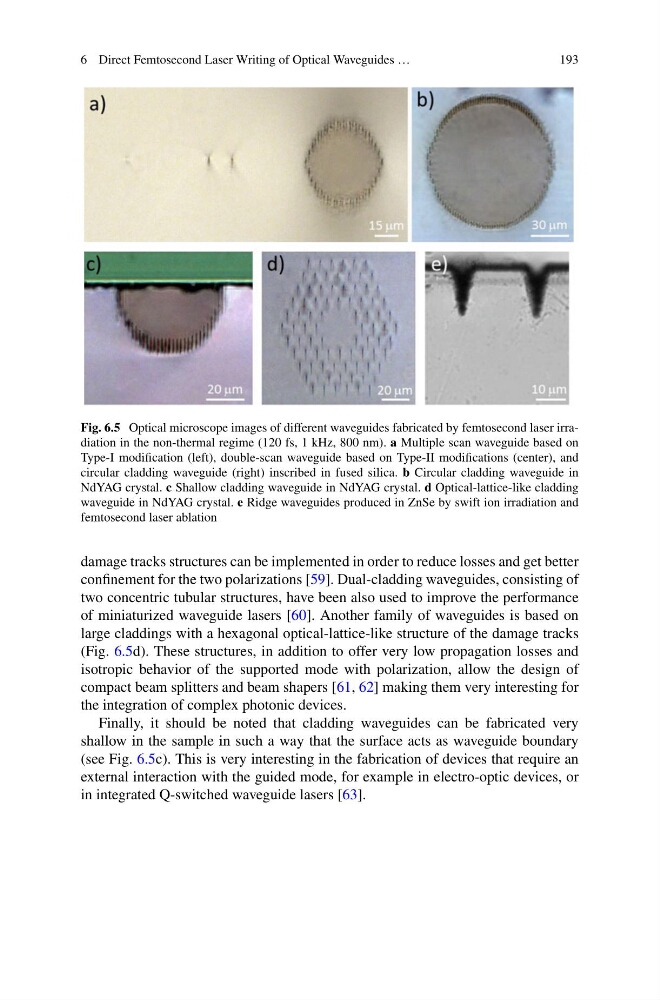
Fig. 6.5 Optical microscope images of different waveguides fabricated by femtosecond laser irradiation in the non-thermal regime (120 fs, 1 kHz, 800 nm). a Multiple scan waveguide based on
Type-I modification (left), double-scan waveguide based on Type-II modifications (center), and
circular cladding waveguide (right) inscribed in fused silica. b Circular cladding waveguide in
NdYAG crystal. c Shallow cladding waveguide in NdYAG crystal. d Optical-lattice-like cladding
waveguide in NdYAG crystal. e Ridge waveguides produced in ZnSe by swift ion irradiation and
femtosecond laser ablation
damage tracks structures can be implemented in order to reduce losses and get better
confinement for the two polarizations [59]. Dual-cladding waveguides, consisting of
two concentric tubular structures, have been also used to improve the performance
of miniaturized waveguide lasers [60]. Another family of waveguides is based on
large claddings with a hexagonal optical-lattice-like structure of the damage tracks
(Fig. 6.5d). These structures, in addition to offer very low propagation losses and
isotropic behavior of the supported mode with polarization, allow the design of
compact beam splitters and beam shapers [61, 62] making them very interesting for
the integration of complex photonic devices.
Finally, it should be noted that cladding waveguides can be fabricated very
shallow in the sample in such a way that the surface acts as waveguide boundary
(see Fig. 6.5c). This is very interesting in the fabrication of devices that require an
external interaction with the guided mode, for example in electro-optic devices, or
in integrated Q-switched waveguide lasers [63].
193
Fig. 6.5 Optical microscope images of different waveguides fabricated by femtosecond laser irradiation in the non-thermal regime (120 fs, 1 kHz, 800 nm). a Multiple scan waveguide based on
Type-I modification (left), double-scan waveguide based on Type-II modifications (center), and
circular cladding waveguide (right) inscribed in fused silica. b Circular cladding waveguide in
NdYAG crystal. c Shallow cladding waveguide in NdYAG crystal. d Optical-lattice-like cladding
waveguide in NdYAG crystal. e Ridge waveguides produced in ZnSe by swift ion irradiation and
femtosecond laser ablation
damage tracks structures can be implemented in order to reduce losses and get better
confinement for the two polarizations [59]. Dual-cladding waveguides, consisting of
two concentric tubular structures, have been also used to improve the performance
of miniaturized waveguide lasers [60]. Another family of waveguides is based on
large claddings with a hexagonal optical-lattice-like structure of the damage tracks
(Fig. 6.5d). These structures, in addition to offer very low propagation losses and
isotropic behavior of the supported mode with polarization, allow the design of
compact beam splitters and beam shapers [61, 62] making them very interesting for
the integration of complex photonic devices.
Finally, it should be noted that cladding waveguides can be fabricated very
shallow in the sample in such a way that the surface acts as waveguide boundary
(see Fig. 6.5c). This is very interesting in the fabrication of devices that require an
external interaction with the guided mode, for example in electro-optic devices, or
in integrated Q-switched waveguide lasers [63].