

186
F. Chen and J. R. V. de Aldana
been used to successfully produce optical waveguides in glasses, single crystals,
ceramics, and organic polymers, showing wide applicability of different materials
[5–7]. In addition, compared with other techniques for waveguide fabrication, direct
femtosecond laser writing possesses powerful three-dimensional (3D) processing
capability of materials, which enables implementation of devices with various functionalities in dielectrics [8]. As a result, highly efficient miniaturized platforms
based on laser-written waveguides have been realized for photonic signal processing
towards diverse purposes [9].
The direct processing of dielectric materials by femtosecond laser contains two
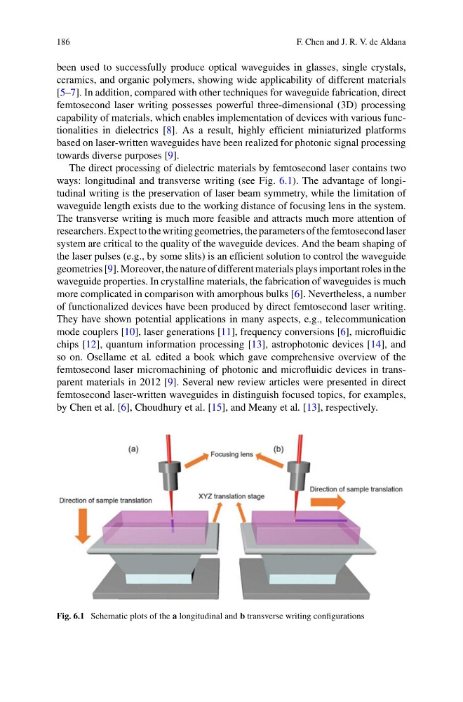
ways: longitudinal and transverse writing (see Fig. 6.1). The advantage of longitudinal writing is the preservation of laser beam symmetry, while the limitation of
waveguide length exists due to the working distance of focusing lens in the system.
The transverse writing is much more feasible and attracts much more attention of
researchers. Expect to the writing geometries, the parameters of the femtosecond laser
system are critical to the quality of the waveguide devices. And the beam shaping of
the laser pulses (e.g., by some slits) is an efficient solution to control the waveguide
geometries [9]. Moreover, the nature of different materials plays important roles in the
waveguide properties. In crystalline materials, the fabrication of waveguides is much
more complicated in comparison with amorphous bulks [6]. Nevertheless, a number
of functionalized devices have been produced by direct femtosecond laser writing.
They have shown potential applications in many aspects, e.g., telecommunication
mode couplers [10], laser generations [11], frequency conversions [6], microfluidic
chips [12], quantum information processing [13], astrophotonic devices [14], and
so on. Osellame et al. edited a book which gave comprehensive overview of the
femtosecond laser micromachining of photonic and microfluidic devices in transparent materials in 2012 [9]. Several new review articles were presented in direct
femtosecond laser-written waveguides in distinguish focused topics, for examples,
by Chen et al. [6], Choudhury et al. [15], and Meany et al. [13], respectively.
Fig. 6.1 Schematic plots of the a longitudinal and b transverse writing configurations
F. Chen and J. R. V. de Aldana
been used to successfully produce optical waveguides in glasses, single crystals,
ceramics, and organic polymers, showing wide applicability of different materials
[5–7]. In addition, compared with other techniques for waveguide fabrication, direct
femtosecond laser writing possesses powerful three-dimensional (3D) processing
capability of materials, which enables implementation of devices with various functionalities in dielectrics [8]. As a result, highly efficient miniaturized platforms
based on laser-written waveguides have been realized for photonic signal processing
towards diverse purposes [9].
The direct processing of dielectric materials by femtosecond laser contains two
ways: longitudinal and transverse writing (see Fig. 6.1). The advantage of longitudinal writing is the preservation of laser beam symmetry, while the limitation of
waveguide length exists due to the working distance of focusing lens in the system.
The transverse writing is much more feasible and attracts much more attention of
researchers. Expect to the writing geometries, the parameters of the femtosecond laser
system are critical to the quality of the waveguide devices. And the beam shaping of
the laser pulses (e.g., by some slits) is an efficient solution to control the waveguide
geometries [9]. Moreover, the nature of different materials plays important roles in the
waveguide properties. In crystalline materials, the fabrication of waveguides is much
more complicated in comparison with amorphous bulks [6]. Nevertheless, a number
of functionalized devices have been produced by direct femtosecond laser writing.
They have shown potential applications in many aspects, e.g., telecommunication
mode couplers [10], laser generations [11], frequency conversions [6], microfluidic
chips [12], quantum information processing [13], astrophotonic devices [14], and
so on. Osellame et al. edited a book which gave comprehensive overview of the
femtosecond laser micromachining of photonic and microfluidic devices in transparent materials in 2012 [9]. Several new review articles were presented in direct
femtosecond laser-written waveguides in distinguish focused topics, for examples,
by Chen et al. [6], Choudhury et al. [15], and Meany et al. [13], respectively.
Fig. 6.1 Schematic plots of the a longitudinal and b transverse writing configurations