

42
3 Simulating Droplet Microfluidic Networks
and decisions as well as simplifications and assumptions during the derivation of
the specification (which provided the basis for the fabricated device) on the actual
behavior.
In the case that those validations show that the behavior has not been implemented as desired, the specification has to be refined, i.e. the dimensions of some
channels, the applied pressures/volumetric flow rates, or some of the used phases
have to be adjusted. In particular, at the beginning of the design process, this of
course is likely needed as assumptions might be inappropriate and simplifications
may have led to an imprecise specification. But then, the entire process of creating
a physical design and fabricating another prototypical device has to be repeated
in order to test again whether the (now refined) design is correct. This iteration of
refining and testing constitutes one of the major drawbacks of today’s design process
as it requires a significant amount of time and resources.
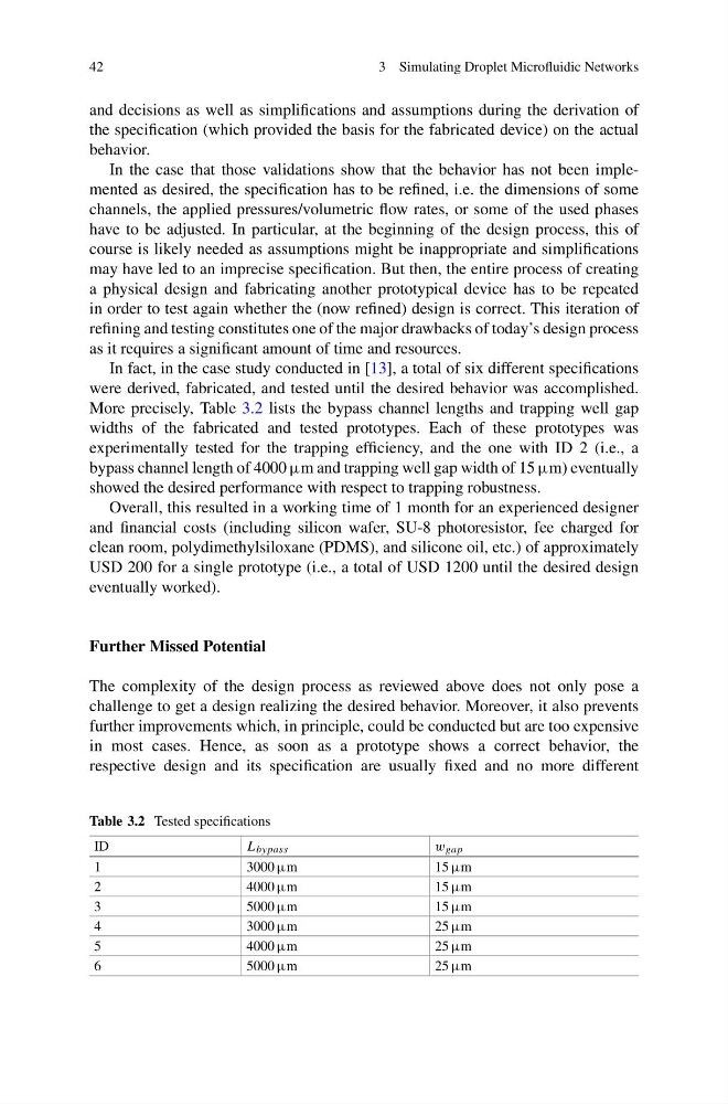
In fact, in the case study conducted in [13], a total of six different specifications
were derived, fabricated, and tested until the desired behavior was accomplished.
More precisely, Table 3.2 lists the bypass channel lengths and trapping well gap
widths of the fabricated and tested prototypes. Each of these prototypes was
experimentally tested for the trapping efficiency, and the one with ID 2 (i.e., a
bypass channel length of 4000 μm and trapping well gap width of 15 μm) eventually
showed the desired performance with respect to trapping robustness.
Overall, this resulted in a working time of 1 month for an experienced designer
and financial costs (including silicon wafer, SU-8 photoresistor, fee charged for
clean room, polydimethylsiloxane (PDMS), and silicone oil, etc.) of approximately
USD 200 for a single prototype (i.e., a total of USD 1200 until the desired design
eventually worked).
Further Missed Potential
The complexity of the design process as reviewed above does not only pose a
challenge to get a design realizing the desired behavior. Moreover, it also prevents
further improvements which, in principle, could be conducted but are too expensive
in most cases. Hence, as soon as a prototype shows a correct behavior, the
respective design and its specification are usually fixed and no more different
Table 3.2 Tested specifications
ID
L bypass
w gap
1
3000 μm
15 μm
2
4000 μm
15 μm
3
5000 μm
15 μm
4
3000 μm
25 μm
5
4000 μm
25 μm
6
5000 μm
25 μm
3 Simulating Droplet Microfluidic Networks
and decisions as well as simplifications and assumptions during the derivation of
the specification (which provided the basis for the fabricated device) on the actual
behavior.
In the case that those validations show that the behavior has not been implemented as desired, the specification has to be refined, i.e. the dimensions of some
channels, the applied pressures/volumetric flow rates, or some of the used phases
have to be adjusted. In particular, at the beginning of the design process, this of
course is likely needed as assumptions might be inappropriate and simplifications
may have led to an imprecise specification. But then, the entire process of creating
a physical design and fabricating another prototypical device has to be repeated
in order to test again whether the (now refined) design is correct. This iteration of
refining and testing constitutes one of the major drawbacks of today’s design process
as it requires a significant amount of time and resources.
In fact, in the case study conducted in [13], a total of six different specifications
were derived, fabricated, and tested until the desired behavior was accomplished.
More precisely, Table 3.2 lists the bypass channel lengths and trapping well gap
widths of the fabricated and tested prototypes. Each of these prototypes was
experimentally tested for the trapping efficiency, and the one with ID 2 (i.e., a
bypass channel length of 4000 μm and trapping well gap width of 15 μm) eventually
showed the desired performance with respect to trapping robustness.
Overall, this resulted in a working time of 1 month for an experienced designer
and financial costs (including silicon wafer, SU-8 photoresistor, fee charged for
clean room, polydimethylsiloxane (PDMS), and silicone oil, etc.) of approximately
USD 200 for a single prototype (i.e., a total of USD 1200 until the desired design
eventually worked).
Further Missed Potential
The complexity of the design process as reviewed above does not only pose a
challenge to get a design realizing the desired behavior. Moreover, it also prevents
further improvements which, in principle, could be conducted but are too expensive
in most cases. Hence, as soon as a prototype shows a correct behavior, the
respective design and its specification are usually fixed and no more different
Table 3.2 Tested specifications
ID
L bypass
w gap
1
3000 μm
15 μm
2
4000 μm
15 μm
3
5000 μm
15 μm
4
3000 μm
25 μm
5
4000 μm
25 μm
6
5000 μm
25 μm