

4.2 Substrate for Epitaxial Growth of III-Nitride LEDs …
37
GaAs substrate: The processing technology of GaAs substrate is also relatively
mature. In addition, GaAs has been widely used in the field of optoelectronics.
However, the epitaxial GaN material on the GaAs substrate shows cubic phase that
has no polarization effect. Furthermore, the cubic phase GaN material is unstable and
can be decomposed at high temperatures. Therefore, there are not so much efforts
from companies and research institutes that use GaAs materials as substrates for
GaN LEDs.
LiAl 2 O 3 substrate: The lattice parameters of the lithium aluminate substrate and
the GaN film are relatively close. The thermal expansion coefficients are also relatively close to each other. Lithium aluminate substrates are suitable for epitaxial GaN
materials, but lithium aluminate is not very stable at high temperatures. The lack of
commercially available large-scale lithium aluminate substrates further limits such
materials for GaN based LED applications.
ZnO substrate: The (0001) plane zinc oxide and gallium nitride have relatively
small lattice mismatch and thermal expansion mismatch. ZnO substrate is transparent and easy to modify the surfaces. Such features make ZnO an ideal alternative
to sapphire substrates. However, zinc oxide substrates can be decomposed at high
temperatures. The thermal stability is in general not ideal. It is also difficult to achieve
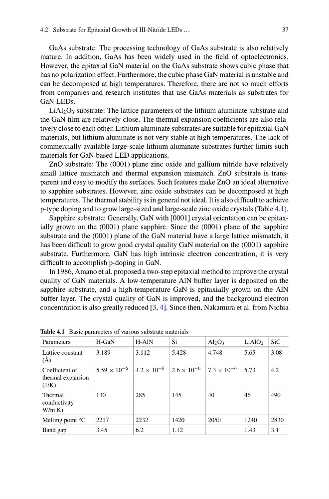
p-type doping and to grow large-sized and large-scale zinc oxide crystals (Table 4.1).
Sapphire substrate: Generally, GaN with [0001] crystal orientation can be epitaxially grown on the (0001) plane sapphire. Since the (0001) plane of the sapphire
substrate and the (0001) plane of the GaN material have a large lattice mismatch, it
has been difficult to grow good crystal quality GaN material on the (0001) sapphire
substrate. Furthermore, GaN has high intrinsic electron concentration, it is very
difficult to accomplish p-doping in GaN.
In 1986, Amano et al. proposed a two-step epitaxial method to improve the crystal
quality of GaN materials. A low-temperature AlN buffer layer is deposited on the
sapphire substrate, and a high-temperature GaN is epitaxially grown on the AlN
buffer layer. The crystal quality of GaN is improved, and the background electron
concentration is also greatly reduced [3, 4]. Since then, Nakamura et al. from Nichia
Table 4.1 Basic parameters of various substrate materials
Parameters
H-GaN
H-AlN
Si
Al 2 O 3
LiAlO 2 SiC
Lattice constant
(Å)
3.189
3.112
5.428
4.748
5.65
3.08
Coefficient of
thermal expansion
(1/K)
5.59 × 10 −6 4.2 × 10 −6 2.6 × 10 −6 7.3 × 10 −6 5.73
4.2
Thermal
conductivity
W/m K)
130
285
145
40
46
490
Melting point °C
2217
2232
1420
2050
1240
2830
Band gap
3.45
6.2
1.12
1.43
3.1
37
GaAs substrate: The processing technology of GaAs substrate is also relatively
mature. In addition, GaAs has been widely used in the field of optoelectronics.
However, the epitaxial GaN material on the GaAs substrate shows cubic phase that
has no polarization effect. Furthermore, the cubic phase GaN material is unstable and
can be decomposed at high temperatures. Therefore, there are not so much efforts
from companies and research institutes that use GaAs materials as substrates for
GaN LEDs.
LiAl 2 O 3 substrate: The lattice parameters of the lithium aluminate substrate and
the GaN film are relatively close. The thermal expansion coefficients are also relatively close to each other. Lithium aluminate substrates are suitable for epitaxial GaN
materials, but lithium aluminate is not very stable at high temperatures. The lack of
commercially available large-scale lithium aluminate substrates further limits such
materials for GaN based LED applications.
ZnO substrate: The (0001) plane zinc oxide and gallium nitride have relatively
small lattice mismatch and thermal expansion mismatch. ZnO substrate is transparent and easy to modify the surfaces. Such features make ZnO an ideal alternative
to sapphire substrates. However, zinc oxide substrates can be decomposed at high
temperatures. The thermal stability is in general not ideal. It is also difficult to achieve
p-type doping and to grow large-sized and large-scale zinc oxide crystals (Table 4.1).
Sapphire substrate: Generally, GaN with [0001] crystal orientation can be epitaxially grown on the (0001) plane sapphire. Since the (0001) plane of the sapphire
substrate and the (0001) plane of the GaN material have a large lattice mismatch, it
has been difficult to grow good crystal quality GaN material on the (0001) sapphire
substrate. Furthermore, GaN has high intrinsic electron concentration, it is very
difficult to accomplish p-doping in GaN.
In 1986, Amano et al. proposed a two-step epitaxial method to improve the crystal
quality of GaN materials. A low-temperature AlN buffer layer is deposited on the
sapphire substrate, and a high-temperature GaN is epitaxially grown on the AlN
buffer layer. The crystal quality of GaN is improved, and the background electron
concentration is also greatly reduced [3, 4]. Since then, Nakamura et al. from Nichia
Table 4.1 Basic parameters of various substrate materials
Parameters
H-GaN
H-AlN
Si
Al 2 O 3
LiAlO 2 SiC
Lattice constant
(Å)
3.189
3.112
5.428
4.748
5.65
3.08
Coefficient of
thermal expansion
(1/K)
5.59 × 10 −6 4.2 × 10 −6 2.6 × 10 −6 7.3 × 10 −6 5.73
4.2
Thermal
conductivity
W/m K)
130
285
145
40
46
490
Melting point °C
2217
2232
1420
2050
1240
2830
Band gap
3.45
6.2
1.12
1.43
3.1