

12.1 GaN-Based Nanorod LED
255
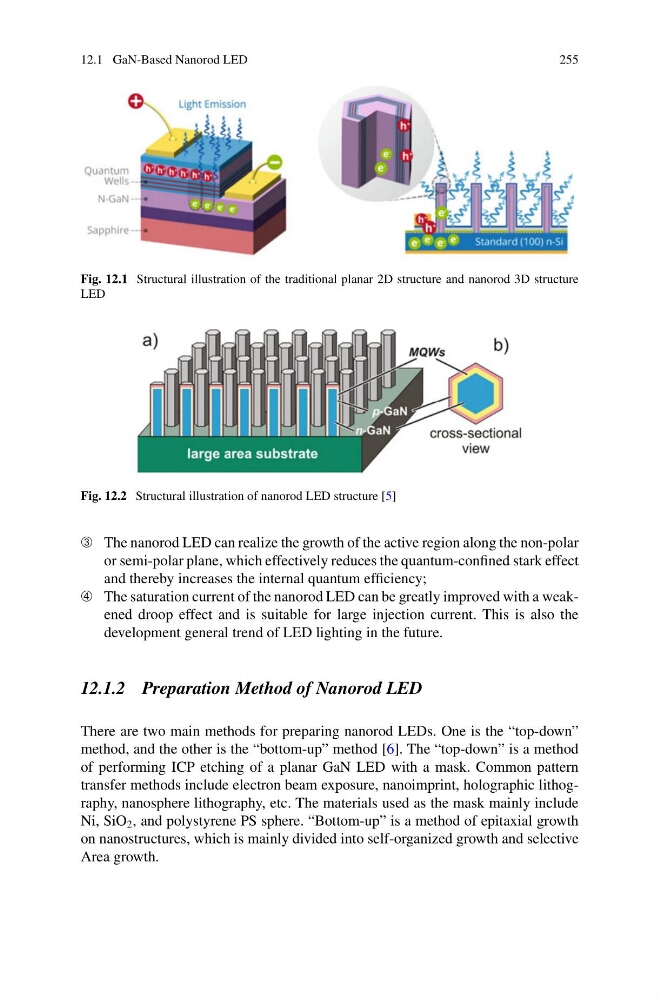
Fig. 12.1 Structural illustration of the traditional planar 2D structure and nanorod 3D structure
LED
Fig. 12.2 Structural illustration of nanorod LED structure [5]
➂ The nanorod LED can realize the growth of the active region along the non-polar
or semi-polar plane, which effectively reduces the quantum-confined stark effect
and thereby increases the internal quantum efficiency;
➃ The saturation current of the nanorod LED can be greatly improved with a weakened droop effect and is suitable for large injection current. This is also the
development general trend of LED lighting in the future.
12.1.2 Preparation Method of Nanorod LED
There are two main methods for preparing nanorod LEDs. One is the “top-down”
method, and the other is the “bottom-up” method [6]. The “top-down” is a method
of performing ICP etching of a planar GaN LED with a mask. Common pattern
transfer methods include electron beam exposure, nanoimprint, holographic lithography, nanosphere lithography, etc. The materials used as the mask mainly include
Ni, SiO 2 , and polystyrene PS sphere. “Bottom-up” is a method of epitaxial growth
on nanostructures, which is mainly divided into self-organized growth and selective
Area growth.
255
Fig. 12.1 Structural illustration of the traditional planar 2D structure and nanorod 3D structure
LED
Fig. 12.2 Structural illustration of nanorod LED structure [5]
➂ The nanorod LED can realize the growth of the active region along the non-polar
or semi-polar plane, which effectively reduces the quantum-confined stark effect
and thereby increases the internal quantum efficiency;
➃ The saturation current of the nanorod LED can be greatly improved with a weakened droop effect and is suitable for large injection current. This is also the
development general trend of LED lighting in the future.
12.1.2 Preparation Method of Nanorod LED
There are two main methods for preparing nanorod LEDs. One is the “top-down”
method, and the other is the “bottom-up” method [6]. The “top-down” is a method
of performing ICP etching of a planar GaN LED with a mask. Common pattern
transfer methods include electron beam exposure, nanoimprint, holographic lithography, nanosphere lithography, etc. The materials used as the mask mainly include
Ni, SiO 2 , and polystyrene PS sphere. “Bottom-up” is a method of epitaxial growth
on nanostructures, which is mainly divided into self-organized growth and selective
Area growth.