

2.1 LED Luminescence Principle
9
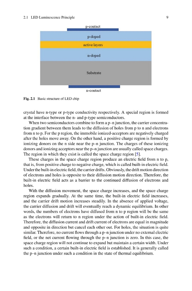
Fig. 2.1 Basic structure of LED chip
crystal have n-type or p-type conductivity respectively. A special region is formed
at the interface between the n- and p-type semiconductors.
When two semiconductors combine to form a p–n junction, the carrier concentration gradient between them leads to the diffusion of holes from p to n and electrons
from n to p. For the p region, the immobile ionized-acceptors are negatively charged
after the holes move away. On the other hand, a positive charge region is formed by
ionizing donors on the n side near the p–n junction. The charges of these ionizing
donors and ionizing acceptors near the p–n junction are usually called space charges.
The region in which they exist is called the space charge region [5].
These charges in the space charge region produce an electric field from n to p,
that is, from positive charge to negative charge, which is called built-in electric field.
Under the built-in electric field, the carrier drifts. Obviously, the drift motion direction
of electrons and holes is opposite to their diffusion motion direction. Therefore, the
built-in electric field acts as a barrier to the continued diffusion of electrons and
holes.
With the diffusion movement, the space charge increases, and the space charge
region expands gradually. At the same time, the built-in electric field increases,
and the carrier drift motion increases steadily. In the absence of applied voltage,
the carrier diffusion and drift will eventually reach a dynamic equilibrium. In other
words, the numbers of electrons have diffused from n to p region will be the same
as the electrons will return to n region under the action of built-in electric field.
Therefore, the diffusion current and drift current of electrons are equal in magnitude
and opposite in direction but cancel each other out. For holes, the situation is quite
similar. Therefore, no current flows through a p–n junction under no external electric
field, or the net current flowing through the p–n junction is zero. In this case, the
space charge region will not continue to expand but maintain a certain width. Under
such a condition, a certain built-in electric field is established. It is generally called
the p–n junction under such a condition in the state of thermal equilibrium.
9
Fig. 2.1 Basic structure of LED chip
crystal have n-type or p-type conductivity respectively. A special region is formed
at the interface between the n- and p-type semiconductors.
When two semiconductors combine to form a p–n junction, the carrier concentration gradient between them leads to the diffusion of holes from p to n and electrons
from n to p. For the p region, the immobile ionized-acceptors are negatively charged
after the holes move away. On the other hand, a positive charge region is formed by
ionizing donors on the n side near the p–n junction. The charges of these ionizing
donors and ionizing acceptors near the p–n junction are usually called space charges.
The region in which they exist is called the space charge region [5].
These charges in the space charge region produce an electric field from n to p,
that is, from positive charge to negative charge, which is called built-in electric field.
Under the built-in electric field, the carrier drifts. Obviously, the drift motion direction
of electrons and holes is opposite to their diffusion motion direction. Therefore, the
built-in electric field acts as a barrier to the continued diffusion of electrons and
holes.
With the diffusion movement, the space charge increases, and the space charge
region expands gradually. At the same time, the built-in electric field increases,
and the carrier drift motion increases steadily. In the absence of applied voltage,
the carrier diffusion and drift will eventually reach a dynamic equilibrium. In other
words, the numbers of electrons have diffused from n to p region will be the same
as the electrons will return to n region under the action of built-in electric field.
Therefore, the diffusion current and drift current of electrons are equal in magnitude
and opposite in direction but cancel each other out. For holes, the situation is quite
similar. Therefore, no current flows through a p–n junction under no external electric
field, or the net current flowing through the p–n junction is zero. In this case, the
space charge region will not continue to expand but maintain a certain width. Under
such a condition, a certain built-in electric field is established. It is generally called
the p–n junction under such a condition in the state of thermal equilibrium.