

192
9 Packaging of Group-III Nitride LED
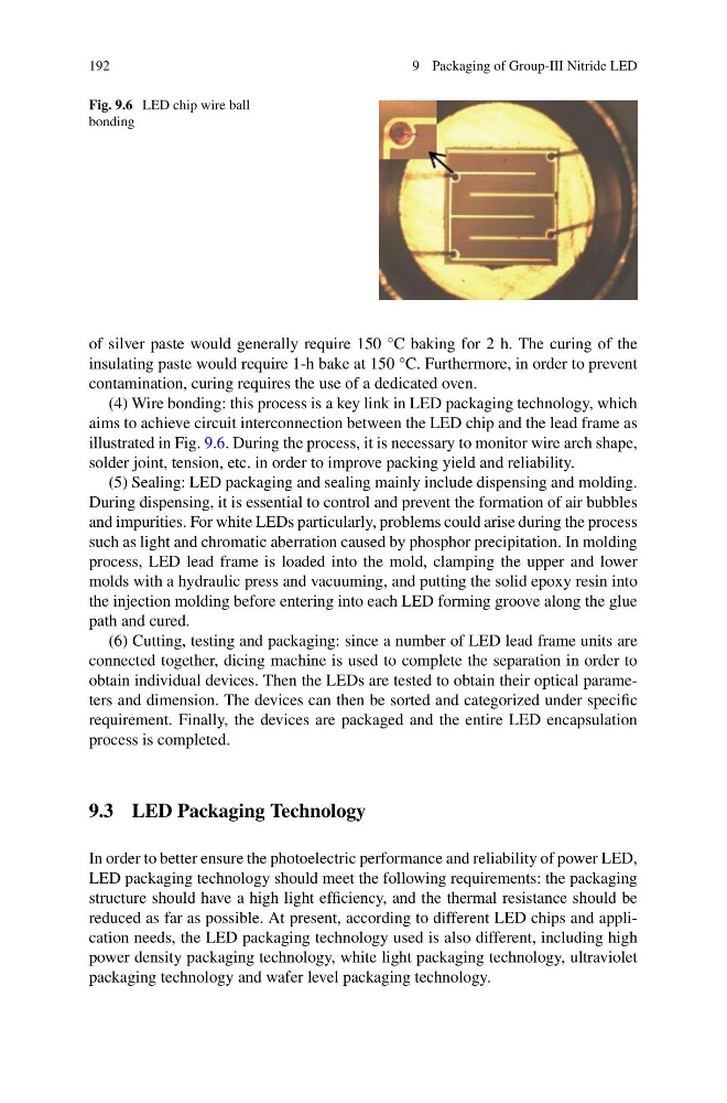
Fig. 9.6 LED chip wire ball
bonding
of silver paste would generally require 150 °C baking for 2 h. The curing of the
insulating paste would require 1-h bake at 150 °C. Furthermore, in order to prevent
contamination, curing requires the use of a dedicated oven.
(4) Wire bonding: this process is a key link in LED packaging technology, which
aims to achieve circuit interconnection between the LED chip and the lead frame as
illustrated in Fig. 9.6. During the process, it is necessary to monitor wire arch shape,
solder joint, tension, etc. in order to improve packing yield and reliability.
(5) Sealing: LED packaging and sealing mainly include dispensing and molding.
During dispensing, it is essential to control and prevent the formation of air bubbles
and impurities. For white LEDs particularly, problems could arise during the process
such as light and chromatic aberration caused by phosphor precipitation. In molding
process, LED lead frame is loaded into the mold, clamping the upper and lower
molds with a hydraulic press and vacuuming, and putting the solid epoxy resin into
the injection molding before entering into each LED forming groove along the glue
path and cured.
(6) Cutting, testing and packaging: since a number of LED lead frame units are
connected together, dicing machine is used to complete the separation in order to
obtain individual devices. Then the LEDs are tested to obtain their optical parameters and dimension. The devices can then be sorted and categorized under specific
requirement. Finally, the devices are packaged and the entire LED encapsulation
process is completed.
9.3 LED Packaging Technology
In order to better ensure the photoelectric performance and reliability of power LED,
LED packaging technology should meet the following requirements: the packaging
structure should have a high light efficiency, and the thermal resistance should be
reduced as far as possible. At present, according to different LED chips and application needs, the LED packaging technology used is also different, including high
power density packaging technology, white light packaging technology, ultraviolet
packaging technology and wafer level packaging technology.
9 Packaging of Group-III Nitride LED
Fig. 9.6 LED chip wire ball
bonding
of silver paste would generally require 150 °C baking for 2 h. The curing of the
insulating paste would require 1-h bake at 150 °C. Furthermore, in order to prevent
contamination, curing requires the use of a dedicated oven.
(4) Wire bonding: this process is a key link in LED packaging technology, which
aims to achieve circuit interconnection between the LED chip and the lead frame as
illustrated in Fig. 9.6. During the process, it is necessary to monitor wire arch shape,
solder joint, tension, etc. in order to improve packing yield and reliability.
(5) Sealing: LED packaging and sealing mainly include dispensing and molding.
During dispensing, it is essential to control and prevent the formation of air bubbles
and impurities. For white LEDs particularly, problems could arise during the process
such as light and chromatic aberration caused by phosphor precipitation. In molding
process, LED lead frame is loaded into the mold, clamping the upper and lower
molds with a hydraulic press and vacuuming, and putting the solid epoxy resin into
the injection molding before entering into each LED forming groove along the glue
path and cured.
(6) Cutting, testing and packaging: since a number of LED lead frame units are
connected together, dicing machine is used to complete the separation in order to
obtain individual devices. Then the LEDs are tested to obtain their optical parameters and dimension. The devices can then be sorted and categorized under specific
requirement. Finally, the devices are packaged and the entire LED encapsulation
process is completed.
9.3 LED Packaging Technology
In order to better ensure the photoelectric performance and reliability of power LED,
LED packaging technology should meet the following requirements: the packaging
structure should have a high light efficiency, and the thermal resistance should be
reduced as far as possible. At present, according to different LED chips and application needs, the LED packaging technology used is also different, including high
power density packaging technology, white light packaging technology, ultraviolet
packaging technology and wafer level packaging technology.