

178
8 III-Nitride LED Chip Fabrication Techniques
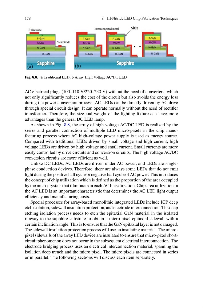
Fig. 8.8. a Traditional LED, b Array High Voltage AC/DC LED
AC electrical plugs (100–110 V/220–230 V) without the need of converters, which
not only significantly reduces the cost of the circuit but also avoids the energy loss
during the power conversion process. AC LEDs can be directly driven by AC drive
through special circuit design. It can operate normally without the need of rectifier
transformer. Therefore, the size and weight of the lighting fixture can have more
advantages than the general DC LED lamp.
As shown in Fig. 8.8, the array of high-voltage AC/DC LED is realized by the
series and parallel connection of multiple LED micro-pixels in the chip manufacturing process where AC high-voltage power supply is used as energy source.
Compared with traditional LEDs driven by small voltage and high current, high
voltage LEDs are driven by high voltage and small current. Small currents are more
easily controlled by drive circuits and conversion circuits. The high voltage AC/DC
conversion circuits are more efficient as well.
Unlike DC LEDs, AC LEDs are driven under AC power, and LEDs are singlephase conduction devices. Therefore, there are always some LEDs that do not emit
light during the positive half cycle or negative half cycle of AC power. This introduces
the concept of chip utilization which is defined as the proportion of the area occupied
by the microcrystals that illuminate in each AC bias direction. Chip area utilization in
the AC LED is an important characteristic that determines the AC LED light output
efficiency and manufacturing costs.
Special processes for array-based monolithic integrated LEDs include ICP deep
etch isolation, sidewall insulation protection, and electrode interconnection. The deep
etching isolation process needs to etch the epitaxial GaN material in the isolated
runway to the sapphire substrate to obtain a micro-pixel epitaxial sidewall with a
certain inclination angle. This is to ensure that the GaN epitaxial layer is not damaged.
The sidewall insulation protection process will use an insulating material. The micropixel sidewalls of the array LED device are insulated to ensure that micro-pixel shortcircuit phenomenon does not occur in the subsequent electrical interconnection. The
electrode bridging process uses an electrical interconnection material, spanning the
isolation deep trench and the micro pixel. The micro pixels are connected in series
or in parallel. The following sections will discuss each item separately.
8 III-Nitride LED Chip Fabrication Techniques
Fig. 8.8. a Traditional LED, b Array High Voltage AC/DC LED
AC electrical plugs (100–110 V/220–230 V) without the need of converters, which
not only significantly reduces the cost of the circuit but also avoids the energy loss
during the power conversion process. AC LEDs can be directly driven by AC drive
through special circuit design. It can operate normally without the need of rectifier
transformer. Therefore, the size and weight of the lighting fixture can have more
advantages than the general DC LED lamp.
As shown in Fig. 8.8, the array of high-voltage AC/DC LED is realized by the
series and parallel connection of multiple LED micro-pixels in the chip manufacturing process where AC high-voltage power supply is used as energy source.
Compared with traditional LEDs driven by small voltage and high current, high
voltage LEDs are driven by high voltage and small current. Small currents are more
easily controlled by drive circuits and conversion circuits. The high voltage AC/DC
conversion circuits are more efficient as well.
Unlike DC LEDs, AC LEDs are driven under AC power, and LEDs are singlephase conduction devices. Therefore, there are always some LEDs that do not emit
light during the positive half cycle or negative half cycle of AC power. This introduces
the concept of chip utilization which is defined as the proportion of the area occupied
by the microcrystals that illuminate in each AC bias direction. Chip area utilization in
the AC LED is an important characteristic that determines the AC LED light output
efficiency and manufacturing costs.
Special processes for array-based monolithic integrated LEDs include ICP deep
etch isolation, sidewall insulation protection, and electrode interconnection. The deep
etching isolation process needs to etch the epitaxial GaN material in the isolated
runway to the sapphire substrate to obtain a micro-pixel epitaxial sidewall with a
certain inclination angle. This is to ensure that the GaN epitaxial layer is not damaged.
The sidewall insulation protection process will use an insulating material. The micropixel sidewalls of the array LED device are insulated to ensure that micro-pixel shortcircuit phenomenon does not occur in the subsequent electrical interconnection. The
electrode bridging process uses an electrical interconnection material, spanning the
isolation deep trench and the micro pixel. The micro pixels are connected in series
or in parallel. The following sections will discuss each item separately.