

8.3 Etching Process
159
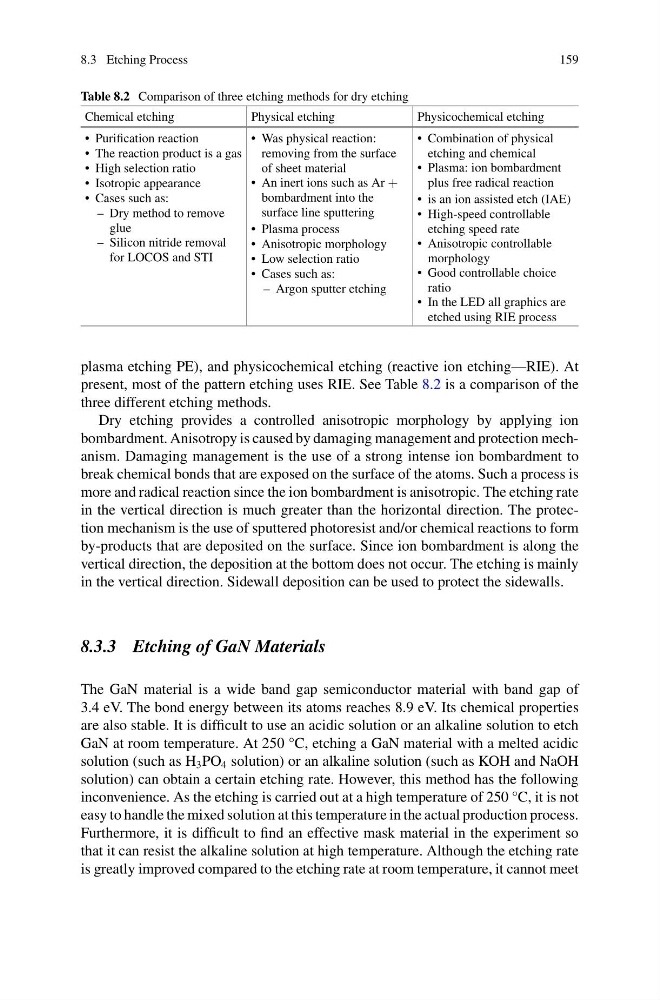
Table 8.2 Comparison of three etching methods for dry etching
Chemical etching
Physical etching
Physicochemical etching
• Purification reaction
• The reaction product is a gas
• High selection ratio
• Isotropic appearance
• Cases such as:
– Dry method to remove
glue
– Silicon nitride removal
for LOCOS and STI
• Was physical reaction:
removing from the surface
of sheet material
• An inert ions such as Ar +
bombardment into the
surface line sputtering
• Plasma process
• Anisotropic morphology
• Low selection ratio
• Cases such as:
– Argon sputter etching
• Combination of physical
etching and chemical
• Plasma: ion bombardment
plus free radical reaction
• is an ion assisted etch (IAE)
• High-speed controllable
etching speed rate
• Anisotropic controllable
morphology
• Good controllable choice
ratio
• In the LED all graphics are
etched using RIE process
plasma etching PE), and physicochemical etching (reactive ion etching—RIE). At
present, most of the pattern etching uses RIE. See Table 8.2 is a comparison of the
three different etching methods.
Dry etching provides a controlled anisotropic morphology by applying ion
bombardment. Anisotropy is caused by damaging management and protection mechanism. Damaging management is the use of a strong intense ion bombardment to
break chemical bonds that are exposed on the surface of the atoms. Such a process is
more and radical reaction since the ion bombardment is anisotropic. The etching rate
in the vertical direction is much greater than the horizontal direction. The protection mechanism is the use of sputtered photoresist and/or chemical reactions to form
by-products that are deposited on the surface. Since ion bombardment is along the
vertical direction, the deposition at the bottom does not occur. The etching is mainly
in the vertical direction. Sidewall deposition can be used to protect the sidewalls.
8.3.3 Etching of GaN Materials
The GaN material is a wide band gap semiconductor material with band gap of
3.4 eV. The bond energy between its atoms reaches 8.9 eV. Its chemical properties
are also stable. It is difficult to use an acidic solution or an alkaline solution to etch
GaN at room temperature. At 250 °C, etching a GaN material with a melted acidic
solution (such as H 3 PO 4 solution) or an alkaline solution (such as KOH and NaOH
solution) can obtain a certain etching rate. However, this method has the following
inconvenience. As the etching is carried out at a high temperature of 250 °C, it is not
easy to handle the mixed solution at this temperature in the actual production process.
Furthermore, it is difficult to find an effective mask material in the experiment so
that it can resist the alkaline solution at high temperature. Although the etching rate
is greatly improved compared to the etching rate at room temperature, it cannot meet
159
Table 8.2 Comparison of three etching methods for dry etching
Chemical etching
Physical etching
Physicochemical etching
• Purification reaction
• The reaction product is a gas
• High selection ratio
• Isotropic appearance
• Cases such as:
– Dry method to remove
glue
– Silicon nitride removal
for LOCOS and STI
• Was physical reaction:
removing from the surface
of sheet material
• An inert ions such as Ar +
bombardment into the
surface line sputtering
• Plasma process
• Anisotropic morphology
• Low selection ratio
• Cases such as:
– Argon sputter etching
• Combination of physical
etching and chemical
• Plasma: ion bombardment
plus free radical reaction
• is an ion assisted etch (IAE)
• High-speed controllable
etching speed rate
• Anisotropic controllable
morphology
• Good controllable choice
ratio
• In the LED all graphics are
etched using RIE process
plasma etching PE), and physicochemical etching (reactive ion etching—RIE). At
present, most of the pattern etching uses RIE. See Table 8.2 is a comparison of the
three different etching methods.
Dry etching provides a controlled anisotropic morphology by applying ion
bombardment. Anisotropy is caused by damaging management and protection mechanism. Damaging management is the use of a strong intense ion bombardment to
break chemical bonds that are exposed on the surface of the atoms. Such a process is
more and radical reaction since the ion bombardment is anisotropic. The etching rate
in the vertical direction is much greater than the horizontal direction. The protection mechanism is the use of sputtered photoresist and/or chemical reactions to form
by-products that are deposited on the surface. Since ion bombardment is along the
vertical direction, the deposition at the bottom does not occur. The etching is mainly
in the vertical direction. Sidewall deposition can be used to protect the sidewalls.
8.3.3 Etching of GaN Materials
The GaN material is a wide band gap semiconductor material with band gap of
3.4 eV. The bond energy between its atoms reaches 8.9 eV. Its chemical properties
are also stable. It is difficult to use an acidic solution or an alkaline solution to etch
GaN at room temperature. At 250 °C, etching a GaN material with a melted acidic
solution (such as H 3 PO 4 solution) or an alkaline solution (such as KOH and NaOH
solution) can obtain a certain etching rate. However, this method has the following
inconvenience. As the etching is carried out at a high temperature of 250 °C, it is not
easy to handle the mixed solution at this temperature in the actual production process.
Furthermore, it is difficult to find an effective mask material in the experiment so
that it can resist the alkaline solution at high temperature. Although the etching rate
is greatly improved compared to the etching rate at room temperature, it cannot meet