

118
7 III-Nitride LED Quantum Efficiency Improvement Technology
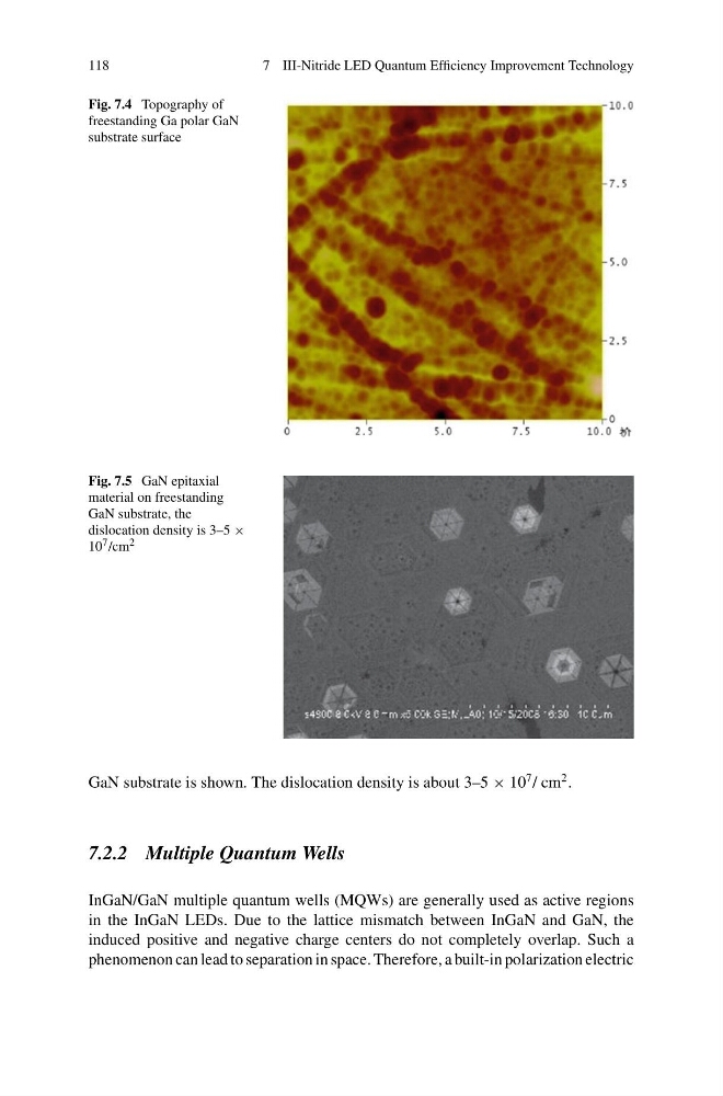
Fig. 7.4 Topography of
freestanding Ga polar GaN
substrate surface
Fig. 7.5 GaN epitaxial
material on freestanding
GaN substrate, the
dislocation density is 3–5 ×
10 7 /cm 2
GaN substrate is shown. The dislocation density is about 3–5 × 10
7 / cm
2 .
7.2.2 Multiple Quantum Wells
InGaN/GaN multiple quantum wells (MQWs) are generally used as active regions
in the InGaN LEDs. Due to the lattice mismatch between InGaN and GaN, the
induced positive and negative charge centers do not completely overlap. Such a
phenomenon can lead to separation in space. Therefore, a built-in polarization electric
7 III-Nitride LED Quantum Efficiency Improvement Technology
Fig. 7.4 Topography of
freestanding Ga polar GaN
substrate surface
Fig. 7.5 GaN epitaxial
material on freestanding
GaN substrate, the
dislocation density is 3–5 ×
10 7 /cm 2
GaN substrate is shown. The dislocation density is about 3–5 × 10
7 / cm
2 .
7.2.2 Multiple Quantum Wells
InGaN/GaN multiple quantum wells (MQWs) are generally used as active regions
in the InGaN LEDs. Due to the lattice mismatch between InGaN and GaN, the
induced positive and negative charge centers do not completely overlap. Such a
phenomenon can lead to separation in space. Therefore, a built-in polarization electric