

158
A. Saha
Source
Drain
Gate
U a
U 0
ΔU
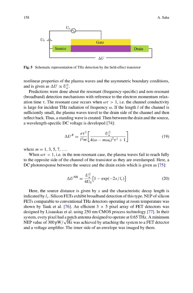
Fig. 5 Schematic representation of THz detection by the field-effect transistor
nonlinear properties of the plasma waves and the asymmetric boundary conditions,
and is given as ∝ U
2
a .
Predictions were done about the resonant (frequency-specific) and non-resonant
(broadband) detection mechanisms with reference to the electron momentum relaxation time τ. The resonant case occurs when ωτ > 1, i.e. the channel conductivity
is large for incident THz radiation of frequency ω. If the length l of the channel is
sufficiently small, the plasma waves travel to the drain side of the channel and then
reflect back. Thus, a standing wave is created. Then between the drain and the source,
a wavelength-specific DC voltage is developed [74]:
R
=
eτ
2
l 2 m
U
2
a
4(ω − mω 0 )
2
τ 2 + 1
(19)
where m = 1, 3, 5, 7, ….
When ωτ < 1, i.e. in the non-resonant case, the plasma waves fail to reach fully
to the opposite side of the channel of the transistor as they are overdamped. Here, a
DC photoresponse between the source and the drain exists which is given as [75]:
NR
=
U
2
a
4U 0
1 − exp(−2x/l c )
(20)
Here, the source distance is given by x and the characteristic decay length is
indicated by l c . Silicon FETs exhibit broadband detection of this type. NEP of silicon
FETs comparable to conventional THz detectors operating at room temperature was
shown by Tauk et al. [76]. An efficient 3 × 5 pixel array of FET detectors was
designed by Lisauskas et al. using 250 nm CMOS process technology [77]. In their
system, every pixel had a patch antenna designed to operate at 0.65 THz. A minimum
NEP value of 300 pW/
√
Hz was achieved by attaching the system to a FET detector
and a voltage amplifier. The inner side of an envelope was imaged by them.
A. Saha
Source
Drain
Gate
U a
U 0
ΔU
Fig. 5 Schematic representation of THz detection by the field-effect transistor
nonlinear properties of the plasma waves and the asymmetric boundary conditions,
and is given as ∝ U
2
a .
Predictions were done about the resonant (frequency-specific) and non-resonant
(broadband) detection mechanisms with reference to the electron momentum relaxation time τ. The resonant case occurs when ωτ > 1, i.e. the channel conductivity
is large for incident THz radiation of frequency ω. If the length l of the channel is
sufficiently small, the plasma waves travel to the drain side of the channel and then
reflect back. Thus, a standing wave is created. Then between the drain and the source,
a wavelength-specific DC voltage is developed [74]:
R
=
eτ
2
l 2 m
U
2
a
4(ω − mω 0 )
2
τ 2 + 1
(19)
where m = 1, 3, 5, 7, ….
When ωτ < 1, i.e. in the non-resonant case, the plasma waves fail to reach fully
to the opposite side of the channel of the transistor as they are overdamped. Here, a
DC photoresponse between the source and the drain exists which is given as [75]:
NR
=
U
2
a
4U 0
1 − exp(−2x/l c )
(20)
Here, the source distance is given by x and the characteristic decay length is
indicated by l c . Silicon FETs exhibit broadband detection of this type. NEP of silicon
FETs comparable to conventional THz detectors operating at room temperature was
shown by Tauk et al. [76]. An efficient 3 × 5 pixel array of FET detectors was
designed by Lisauskas et al. using 250 nm CMOS process technology [77]. In their
system, every pixel had a patch antenna designed to operate at 0.65 THz. A minimum
NEP value of 300 pW/
√
Hz was achieved by attaching the system to a FET detector
and a voltage amplifier. The inner side of an envelope was imaged by them.