

Heterostructure Devices for THz Signal Recognition
109
2 Imaging with Sensing Technique of Terahertz Utilizing
III–V HEMTs
2.1 Device Manufacturing
HEMT manufactured with gallium arsenide-supported hetero-structure material is
commonly used for recognition/discharge of THz radiation [3, 4]. In order to achieve
an enhanced responsivity and recognition sensitivity to Terahertz radiation, most
of the researchers initiate InAlAs/InGaAs HEMT on an InP substrate arrangement
[10]. Here 80-nm length of gate region of a HEMT manufactured affords a unitygain cutoff frequency (f τ ) of 298 GHz with a transconductance (g m ) of 700 mS/mm
[11]. High electron mobility transistor is focused toward 0.3-THz, 2-mW radiation
to distinguish the recognition belongings. Gold-made ribbon wires for pad-covering
interconnect may perform like antenna.
2.2 Demonstrations for Imaging and Sensing of Terahertz
Primarily, the sensitivity due to recognition of high electron mobility transistor was
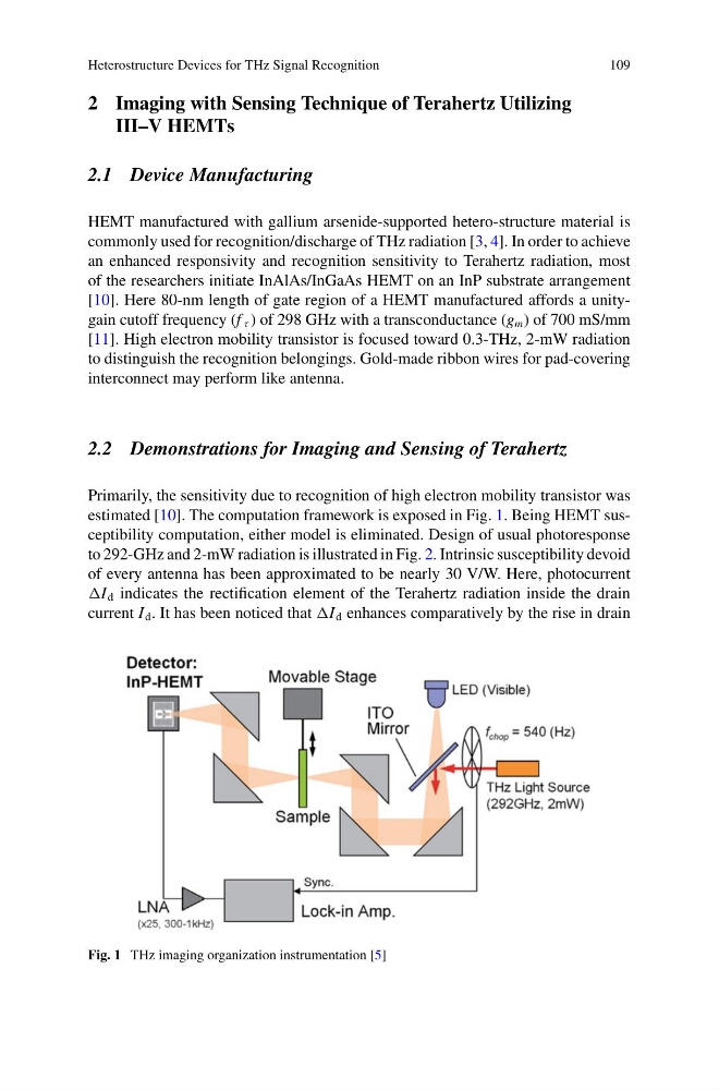
estimated [10]. The computation framework is exposed in Fig. 1. Being HEMT susceptibility computation, either model is eliminated. Design of usual photoresponse
to 292-GHz and 2-mW radiation is illustrated in Fig. 2. Intrinsic susceptibility devoid
of every antenna has been approximated to be nearly 30 V/W. Here, photocurrent
I d indicates the rectification element of the Terahertz radiation inside the drain
current I d . It has been noticed that I d enhances comparatively by the rise in drain
Fig. 1 THz imaging organization instrumentation [5]
109
2 Imaging with Sensing Technique of Terahertz Utilizing
III–V HEMTs
2.1 Device Manufacturing
HEMT manufactured with gallium arsenide-supported hetero-structure material is
commonly used for recognition/discharge of THz radiation [3, 4]. In order to achieve
an enhanced responsivity and recognition sensitivity to Terahertz radiation, most
of the researchers initiate InAlAs/InGaAs HEMT on an InP substrate arrangement
[10]. Here 80-nm length of gate region of a HEMT manufactured affords a unitygain cutoff frequency (f τ ) of 298 GHz with a transconductance (g m ) of 700 mS/mm
[11]. High electron mobility transistor is focused toward 0.3-THz, 2-mW radiation
to distinguish the recognition belongings. Gold-made ribbon wires for pad-covering
interconnect may perform like antenna.
2.2 Demonstrations for Imaging and Sensing of Terahertz
Primarily, the sensitivity due to recognition of high electron mobility transistor was
estimated [10]. The computation framework is exposed in Fig. 1. Being HEMT susceptibility computation, either model is eliminated. Design of usual photoresponse
to 292-GHz and 2-mW radiation is illustrated in Fig. 2. Intrinsic susceptibility devoid
of every antenna has been approximated to be nearly 30 V/W. Here, photocurrent
I d indicates the rectification element of the Terahertz radiation inside the drain
current I d . It has been noticed that I d enhances comparatively by the rise in drain
Fig. 1 THz imaging organization instrumentation [5]