

212
M. Sakamoto et al.
[2], represents a vast source of untapped energy. Developing artificial IR-light-to-fuel
conversion systems would open up this resource for applications. However, despite
extensive research efforts, conversion of IR-light to chemical energy remains challenging. Although certain narrow bandgap semiconductors, such as HgCdTe and
InGaAs are known to be effective IR-light-absorbing materials, the high toxicity,
low electromotive force, and poor stability of these materials have restricted their
applications as photocatalysts [3, 4].
Localized surface plasmon resonance (LSPR) is a phenomenon related to collective oscillation of free carriers in nanomaterials, which can be applied to overcome the limitations of harvesting solar energy in the IR region [5–16]. Recently,
copper chalcogenide nanocrystals (NCs) have drawn interest as a novel series of
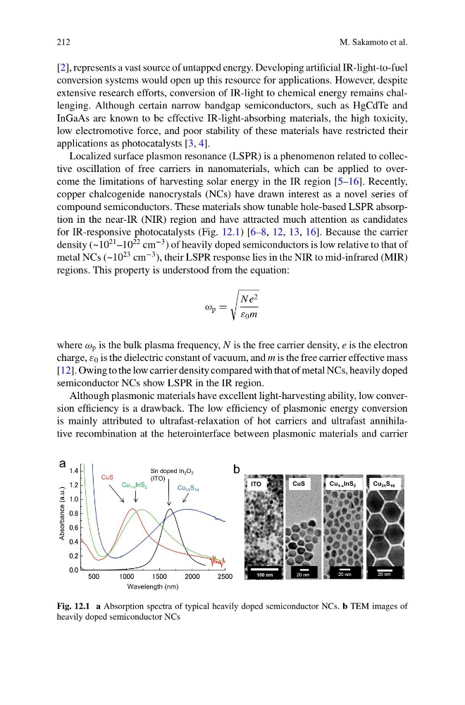
compound semiconductors. These materials show tunable hole-based LSPR absorption in the near-IR (NIR) region and have attracted much attention as candidates
for IR-responsive photocatalysts (Fig. 12.1) [6–8, 12, 13, 16]. Because the carrier
density (~10
21 –10
22 cm
−3 ) of heavily doped semiconductors is low relative to that of
metal NCs (~10
23 cm
−3 ), their LSPR response lies in the NIR to mid-infrared (MIR)
regions. This property is understood from the equation:
ω p =
N e 2
ε 0 m
where ω p is the bulk plasma frequency, N is the free carrier density, e is the electron
charge, ε 0 is the dielectric constant of vacuum, and m is the free carrier effective mass
[12]. Owing to the low carrier density compared with that of metal NCs, heavily doped
semiconductor NCs show LSPR in the IR region.
Although plasmonic materials have excellent light-harvesting ability, low conversion efficiency is a drawback. The low efficiency of plasmonic energy conversion
is mainly attributed to ultrafast-relaxation of hot carriers and ultrafast annihilative recombination at the heterointerface between plasmonic materials and carrier
Fig. 12.1 a Absorption spectra of typical heavily doped semiconductor NCs. b TEM images of
heavily doped semiconductor NCs
M. Sakamoto et al.
[2], represents a vast source of untapped energy. Developing artificial IR-light-to-fuel
conversion systems would open up this resource for applications. However, despite
extensive research efforts, conversion of IR-light to chemical energy remains challenging. Although certain narrow bandgap semiconductors, such as HgCdTe and
InGaAs are known to be effective IR-light-absorbing materials, the high toxicity,
low electromotive force, and poor stability of these materials have restricted their
applications as photocatalysts [3, 4].
Localized surface plasmon resonance (LSPR) is a phenomenon related to collective oscillation of free carriers in nanomaterials, which can be applied to overcome the limitations of harvesting solar energy in the IR region [5–16]. Recently,
copper chalcogenide nanocrystals (NCs) have drawn interest as a novel series of
compound semiconductors. These materials show tunable hole-based LSPR absorption in the near-IR (NIR) region and have attracted much attention as candidates
for IR-responsive photocatalysts (Fig. 12.1) [6–8, 12, 13, 16]. Because the carrier
density (~10
21 –10
22 cm
−3 ) of heavily doped semiconductors is low relative to that of
metal NCs (~10
23 cm
−3 ), their LSPR response lies in the NIR to mid-infrared (MIR)
regions. This property is understood from the equation:
ω p =
N e 2
ε 0 m
where ω p is the bulk plasma frequency, N is the free carrier density, e is the electron
charge, ε 0 is the dielectric constant of vacuum, and m is the free carrier effective mass
[12]. Owing to the low carrier density compared with that of metal NCs, heavily doped
semiconductor NCs show LSPR in the IR region.
Although plasmonic materials have excellent light-harvesting ability, low conversion efficiency is a drawback. The low efficiency of plasmonic energy conversion
is mainly attributed to ultrafast-relaxation of hot carriers and ultrafast annihilative recombination at the heterointerface between plasmonic materials and carrier
Fig. 12.1 a Absorption spectra of typical heavily doped semiconductor NCs. b TEM images of
heavily doped semiconductor NCs