

1 Introduction
5
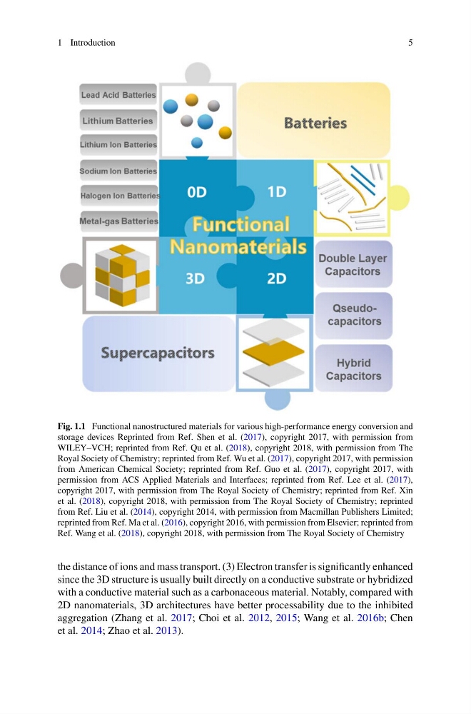
Fig. 1.1 Functional nanostructured materials for various high-performance energy conversion and
storage devices Reprinted from Ref. Shen et al. (2017), copyright 2017, with permission from
WILEY–VCH; reprinted from Ref. Qu et al. (2018), copyright 2018, with permission from The
Royal Society of Chemistry; reprinted from Ref. Wu et al. (2017), copyright 2017, with permission
from American Chemical Society; reprinted from Ref. Guo et al. (2017), copyright 2017, with
permission from ACS Applied Materials and Interfaces; reprinted from Ref. Lee et al. (2017),
copyright 2017, with permission from The Royal Society of Chemistry; reprinted from Ref. Xin
et al. (2018), copyright 2018, with permission from The Royal Society of Chemistry; reprinted
from Ref. Liu et al. (2014), copyright 2014, with permission from Macmillan Publishers Limited;
reprinted from Ref. Ma et al. (2016), copyright 2016, with permission from Elsevier; reprinted from
Ref. Wang et al. (2018), copyright 2018, with permission from The Royal Society of Chemistry
the distance of ions and mass transport. (3) Electron transfer is significantly enhanced
since the 3D structure is usually built directly on a conductive substrate or hybridized
with a conductive material such as a carbonaceous material. Notably, compared with
2D nanomaterials, 3D architectures have better processability due to the inhibited
aggregation (Zhang et al. 2017; Choi et al. 2012, 2015; Wang et al. 2016b; Chen
et al. 2014; Zhao et al. 2013).
5
Fig. 1.1 Functional nanostructured materials for various high-performance energy conversion and
storage devices Reprinted from Ref. Shen et al. (2017), copyright 2017, with permission from
WILEY–VCH; reprinted from Ref. Qu et al. (2018), copyright 2018, with permission from The
Royal Society of Chemistry; reprinted from Ref. Wu et al. (2017), copyright 2017, with permission
from American Chemical Society; reprinted from Ref. Guo et al. (2017), copyright 2017, with
permission from ACS Applied Materials and Interfaces; reprinted from Ref. Lee et al. (2017),
copyright 2017, with permission from The Royal Society of Chemistry; reprinted from Ref. Xin
et al. (2018), copyright 2018, with permission from The Royal Society of Chemistry; reprinted
from Ref. Liu et al. (2014), copyright 2014, with permission from Macmillan Publishers Limited;
reprinted from Ref. Ma et al. (2016), copyright 2016, with permission from Elsevier; reprinted from
Ref. Wang et al. (2018), copyright 2018, with permission from The Royal Society of Chemistry
the distance of ions and mass transport. (3) Electron transfer is significantly enhanced
since the 3D structure is usually built directly on a conductive substrate or hybridized
with a conductive material such as a carbonaceous material. Notably, compared with
2D nanomaterials, 3D architectures have better processability due to the inhibited
aggregation (Zhang et al. 2017; Choi et al. 2012, 2015; Wang et al. 2016b; Chen
et al. 2014; Zhao et al. 2013).