

Characterization Techniques in Nanotechnology …
61
(a)
h
w
VH
e
-
B
B
F
v
Lorentz force
z
x
y
Coordinate
system
I
V = 0
(b)
VH= V24
3
1
2
4
V
A
I13
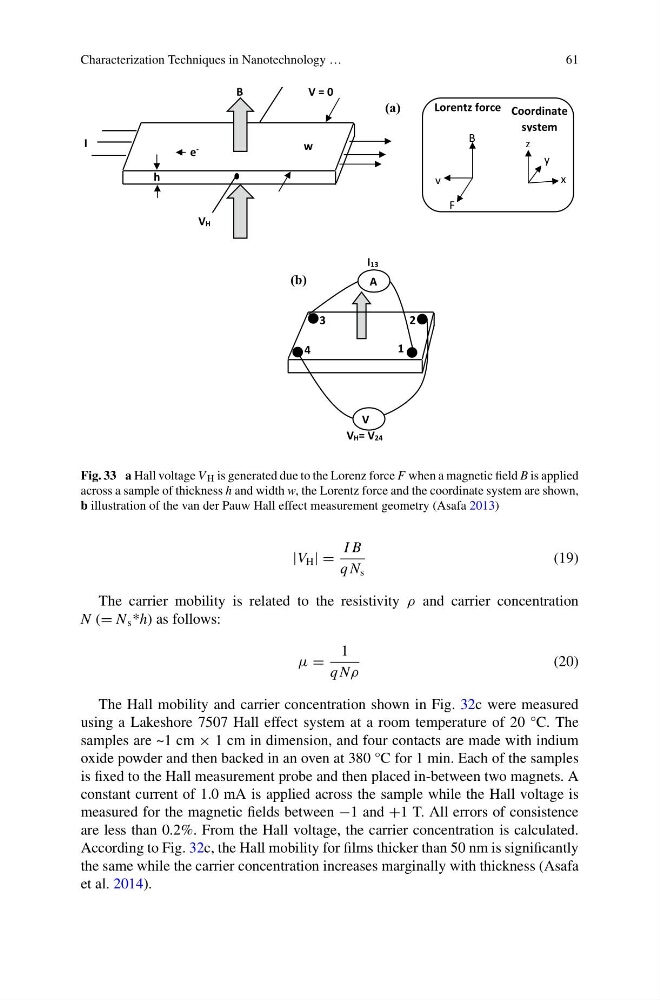
Fig. 33 a Hall voltage V H is generated due to the Lorenz force F when a magnetic field B is applied
across a sample of thickness h and width w, the Lorentz force and the coordinate system are shown,
b illustration of the van der Pauw Hall effect measurement geometry (Asafa 2013)
|V H | =
I B
q N s
(19)
The carrier mobility is related to the resistivity ρ and carrier concentration
N (= N s *h) as follows:
μ =
1
q Nρ
(20)
The Hall mobility and carrier concentration shown in Fig. 32c were measured
using a Lakeshore 7507 Hall effect system at a room temperature of 20 °C. The
samples are ~1 cm × 1 cm in dimension, and four contacts are made with indium
oxide powder and then backed in an oven at 380 °C for 1 min. Each of the samples
is fixed to the Hall measurement probe and then placed in-between two magnets. A
constant current of 1.0 mA is applied across the sample while the Hall voltage is
measured for the magnetic fields between −1 and +1 T. All errors of consistence
are less than 0.2%. From the Hall voltage, the carrier concentration is calculated.
According to Fig. 32c, the Hall mobility for films thicker than 50 nm is significantly
the same while the carrier concentration increases marginally with thickness (Asafa
et al. 2014).
61
(a)
h
w
VH
e
-
B
B
F
v
Lorentz force
z
x
y
Coordinate
system
I
V = 0
(b)
VH= V24
3
1
2
4
V
A
I13
Fig. 33 a Hall voltage V H is generated due to the Lorenz force F when a magnetic field B is applied
across a sample of thickness h and width w, the Lorentz force and the coordinate system are shown,
b illustration of the van der Pauw Hall effect measurement geometry (Asafa 2013)
|V H | =
I B
q N s
(19)
The carrier mobility is related to the resistivity ρ and carrier concentration
N (= N s *h) as follows:
μ =
1
q Nρ
(20)
The Hall mobility and carrier concentration shown in Fig. 32c were measured
using a Lakeshore 7507 Hall effect system at a room temperature of 20 °C. The
samples are ~1 cm × 1 cm in dimension, and four contacts are made with indium
oxide powder and then backed in an oven at 380 °C for 1 min. Each of the samples
is fixed to the Hall measurement probe and then placed in-between two magnets. A
constant current of 1.0 mA is applied across the sample while the Hall voltage is
measured for the magnetic fields between −1 and +1 T. All errors of consistence
are less than 0.2%. From the Hall voltage, the carrier concentration is calculated.
According to Fig. 32c, the Hall mobility for films thicker than 50 nm is significantly
the same while the carrier concentration increases marginally with thickness (Asafa
et al. 2014).