

139
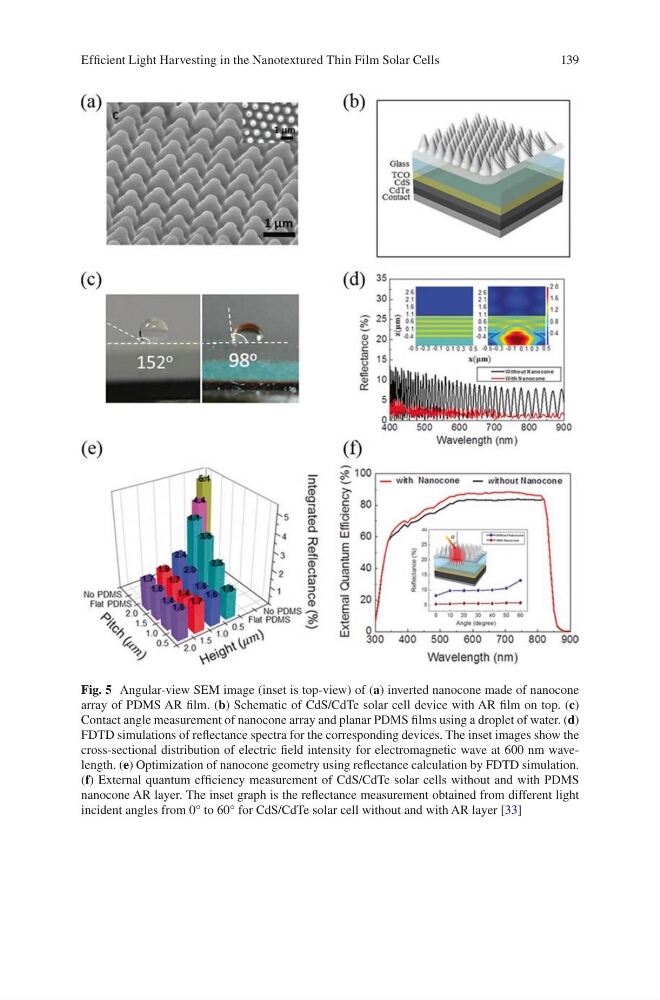
Fig. 5 Angular-view SEM image (inset is top-view) of (a) inverted nanocone made of nanocone
array of PDMS AR film. (b) Schematic of CdS/CdTe solar cell device with AR film on top. (c)
Contact angle measurement of nanocone array and planar PDMS films using a droplet of water. (d)
FDTD simulations of reflectance spectra for the corresponding devices. The inset images show the
cross-sectional distribution of electric field intensity for electromagnetic wave at 600 nm wavelength. (e) Optimization of nanocone geometry using reflectance calculation by FDTD simulation.
(f) External quantum efficiency measurement of CdS/CdTe solar cells without and with PDMS
nanocone AR layer. The inset graph is the reflectance measurement obtained from different light
incident angles from 0° to 60° for CdS/CdTe solar cell without and with AR layer [33]
Efficient Light Harvesting in the Nanotextured Thin Film Solar Cells
Fig. 5 Angular-view SEM image (inset is top-view) of (a) inverted nanocone made of nanocone
array of PDMS AR film. (b) Schematic of CdS/CdTe solar cell device with AR film on top. (c)
Contact angle measurement of nanocone array and planar PDMS films using a droplet of water. (d)
FDTD simulations of reflectance spectra for the corresponding devices. The inset images show the
cross-sectional distribution of electric field intensity for electromagnetic wave at 600 nm wavelength. (e) Optimization of nanocone geometry using reflectance calculation by FDTD simulation.
(f) External quantum efficiency measurement of CdS/CdTe solar cells without and with PDMS
nanocone AR layer. The inset graph is the reflectance measurement obtained from different light
incident angles from 0° to 60° for CdS/CdTe solar cell without and with AR layer [33]
Efficient Light Harvesting in the Nanotextured Thin Film Solar Cells