

1
0.8
0.6
0.4
0.2
0
500
550
600
650
Wavelength (nm)
Fraction scattered into substrate
750
700
50
10
|E| 2
8
6
4
2
0
50
-50
-50
0
0
λ = 850 nm
y position (nm)
x position (nm)
Dipole
Cylinder
Hemisphere
Sphere 100 nm
Sphere 150 nm
800
0
20
400
External quantum efficiency
(%)
Current density (mA cm
–2
)
600
Nano 10-µm-thick Si
Planar 10-µm-thick Si w/AR layer
Nano 10-µm-thick Si
Planar 10-µm-thick Si w/AR layer
800
Wavelength (nm)
1,000
0
0.2
Voltage (V)
AI
p + -Si
n + -Si
n-Si
SiO 2
0.4
0.6
40
60
80
100
0
10
20
30
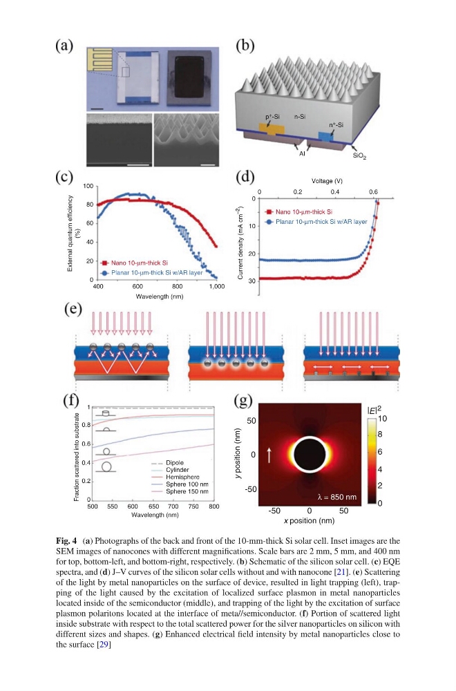
Fig. 4 (a) Photographs of the back and front of the 10-mm-thick Si solar cell. Inset images are the
SEM images of nanocones with different magnifications. Scale bars are 2 mm, 5 mm, and 400 nm
for top, bottom-left, and bottom-right, respectively. (b) Schematic of the silicon solar cell. (c) EQE
spectra, and (d) J–V curves of the silicon solar cells without and with nanocone [21]. (e) Scattering
of the light by metal nanoparticles on the surface of device, resulted in light trapping (left), trapping of the light caused by the excitation of localized surface plasmon in metal nanoparticles
located inside of the semiconductor (middle), and trapping of the light by the excitation of surface
plasmon polaritons located at the interface of meta//semiconductor. (f) Portion of scattered light
inside substrate with respect to the total scattered power for the silver nanoparticles on silicon with
different sizes and shapes. (g) Enhanced electrical field intensity by metal nanoparticles close to
the surface [29]
0.8
0.6
0.4
0.2
0
500
550
600
650
Wavelength (nm)
Fraction scattered into substrate
750
700
50
10
|E| 2
8
6
4
2
0
50
-50
-50
0
0
λ = 850 nm
y position (nm)
x position (nm)
Dipole
Cylinder
Hemisphere
Sphere 100 nm
Sphere 150 nm
800
0
20
400
External quantum efficiency
(%)
Current density (mA cm
–2
)
600
Nano 10-µm-thick Si
Planar 10-µm-thick Si w/AR layer
Nano 10-µm-thick Si
Planar 10-µm-thick Si w/AR layer
800
Wavelength (nm)
1,000
0
0.2
Voltage (V)
AI
p + -Si
n + -Si
n-Si
SiO 2
0.4
0.6
40
60
80
100
0
10
20
30
Fig. 4 (a) Photographs of the back and front of the 10-mm-thick Si solar cell. Inset images are the
SEM images of nanocones with different magnifications. Scale bars are 2 mm, 5 mm, and 400 nm
for top, bottom-left, and bottom-right, respectively. (b) Schematic of the silicon solar cell. (c) EQE
spectra, and (d) J–V curves of the silicon solar cells without and with nanocone [21]. (e) Scattering
of the light by metal nanoparticles on the surface of device, resulted in light trapping (left), trapping of the light caused by the excitation of localized surface plasmon in metal nanoparticles
located inside of the semiconductor (middle), and trapping of the light by the excitation of surface
plasmon polaritons located at the interface of meta//semiconductor. (f) Portion of scattered light
inside substrate with respect to the total scattered power for the silver nanoparticles on silicon with
different sizes and shapes. (g) Enhanced electrical field intensity by metal nanoparticles close to
the surface [29]