

enhance photocatalytic efficiency (Li et al. 2015b, 2017c; Ong et al. 2016) using
improved synthetic methods (Che et al. 2017; Li et al. 2017b), design of electronical
structure (Ran et al. 2018b; Wei et al. 2018a; Wu et al. 2019), and nanostructure
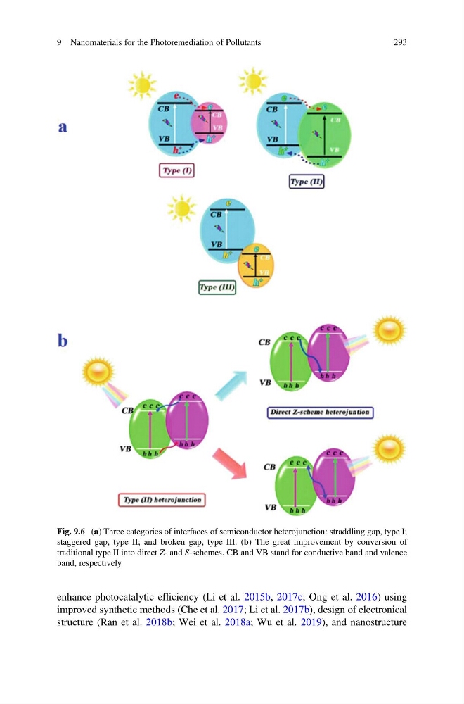
Fig. 9.6 (a) Three categories of interfaces of semiconductor heterojunction: straddling gap, type I;
staggered gap, type II; and broken gap, type III. (b) The great improvement by conversion of
traditional type II into direct Z- and S-schemes. CB and VB stand for conductive band and valence
band, respectively
9 Nanomaterials for the Photoremediation of Pollutants
293
improved synthetic methods (Che et al. 2017; Li et al. 2017b), design of electronical
structure (Ran et al. 2018b; Wei et al. 2018a; Wu et al. 2019), and nanostructure
Fig. 9.6 (a) Three categories of interfaces of semiconductor heterojunction: straddling gap, type I;
staggered gap, type II; and broken gap, type III. (b) The great improvement by conversion of
traditional type II into direct Z- and S-schemes. CB and VB stand for conductive band and valence
band, respectively
9 Nanomaterials for the Photoremediation of Pollutants
293