

406
A. Mishra
scanning Kelvin probe microscopy (SKPM) measurement, which revealed the PFN
interlayer can effectively prevent the built-up of space charge under light, thus have
a strong impact on the charge carrier transport. The PFN layer formed a microscopic
electric dipole and the direction of the dipole was aligned with the V bi .
Han et al. used ZnO/PFN bilayer as CIL in which the ZnO nanoparticles can
function as an efficient ETL to reduce series resistance, while the PFN can improve
the energy level alignment through the formation of an interfacial dipole between
ZnO and photoactive layer. The inverted device gave high performance using bilayer
ZnO/PFN compared to only ZnO or PFN-based devices (Han et al. 2016).
Guo et al. demonstrated an enhancement of the OSC performance with ternary
PEI/SnO 2 /PFN composite interlayer by modulating the energy level between the
active layer and electrode and reduced the interfacial defects (Guo et al. 2019). The
inverted device using this ternary interlayer led to a dramatic increase in the device
performance with PCE of 7.18% compared to 5.5% larger shunt resistance (R sh ) and
a decrease of series or contact resistance (R s ) were observed, which could prevent
the leakage current, resulting in the increased J SC and FF.
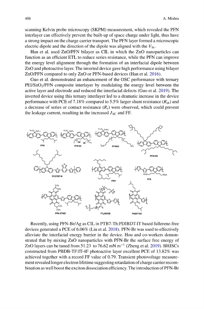
Recently, using PFN-Br/Ag as CIL in PTB7-Th:PDIBDT-IT based fullerene-free
devices generated a PCE of 6.06% (Liu et al. 2018). PFN-Br was used to effectively
alleviate the interfacial energy barrier in the device. Hou and co-workers demonstrated that by mixing ZnO nanoparticles with PFN-Br the surface free energy of
ZnO layers can be tuned from 51.23 to 76.62 mN m
−1 (Zheng et al. 2019). BHJSCs
constructed from PBDB-TF:IT-4F photoactive layer excellent PCE of 13.82% was
achieved together with a record FF value of 0.79. Transient photovoltage measurement revealed longer electron lifetime suggesting retardation of charge carrier recombination as well boost the exciton dissociation efficiency. The introduction of PFN-Br
A. Mishra
scanning Kelvin probe microscopy (SKPM) measurement, which revealed the PFN
interlayer can effectively prevent the built-up of space charge under light, thus have
a strong impact on the charge carrier transport. The PFN layer formed a microscopic
electric dipole and the direction of the dipole was aligned with the V bi .
Han et al. used ZnO/PFN bilayer as CIL in which the ZnO nanoparticles can
function as an efficient ETL to reduce series resistance, while the PFN can improve
the energy level alignment through the formation of an interfacial dipole between
ZnO and photoactive layer. The inverted device gave high performance using bilayer
ZnO/PFN compared to only ZnO or PFN-based devices (Han et al. 2016).
Guo et al. demonstrated an enhancement of the OSC performance with ternary
PEI/SnO 2 /PFN composite interlayer by modulating the energy level between the
active layer and electrode and reduced the interfacial defects (Guo et al. 2019). The
inverted device using this ternary interlayer led to a dramatic increase in the device
performance with PCE of 7.18% compared to 5.5% larger shunt resistance (R sh ) and
a decrease of series or contact resistance (R s ) were observed, which could prevent
the leakage current, resulting in the increased J SC and FF.
Recently, using PFN-Br/Ag as CIL in PTB7-Th:PDIBDT-IT based fullerene-free
devices generated a PCE of 6.06% (Liu et al. 2018). PFN-Br was used to effectively
alleviate the interfacial energy barrier in the device. Hou and co-workers demonstrated that by mixing ZnO nanoparticles with PFN-Br the surface free energy of
ZnO layers can be tuned from 51.23 to 76.62 mN m
−1 (Zheng et al. 2019). BHJSCs
constructed from PBDB-TF:IT-4F photoactive layer excellent PCE of 13.82% was
achieved together with a record FF value of 0.79. Transient photovoltage measurement revealed longer electron lifetime suggesting retardation of charge carrier recombination as well boost the exciton dissociation efficiency. The introduction of PFN-Br