

15 Yet to Be Challenged: TiO 2 as the Photo-Anode Material …
291
to the inefficient charge transport of electrons through the TiO 2 film, due to the pores
of the film, causing recombination reactions before being collected (Pichot et al.
2000).
Another reason for optimizing the layer structure of TiO 2 is to lessen the grain
boundaries of the material. This allows for faster transport of charges and lower
recombination. Yu et al. lowered the thickness of the mesoporous layer from the
conventional 10 μm, to 300 nm, leading to recombination only at the surface, and
eliminating recombination with the oxidized dye and redox electrolyte. An added
advantage was that at these thicknesses, the localized surface plasmon created at the
FTO/TiO 2 interface was able to induce a relatively strong electric field at the TiO 2 /dye
interface, enhancing light absorption by the dyes and increasing cell efficiency. However, in this study, oxygen vacancy-Ti
3+ type surface defects were formed, decreasing the efficiency almost linearly with the increased concentration of Ti
3+ (Tributsch
2004). Defects can serve as recombination centers and pathways for electron back
transfer, and decreased V OC and FF. The lower efficiency can also be attributed to
the lower dye adsorption, due to the smaller mesoporous layer, leading to a lower
J SC (Yu et al. 2012).
To address both the surface area and grain boundaries, several groups have investigated fabricating TiO 2 in nanostructures to yield materials with fewer grain boundaries, and well-defined conduction pathways. These materials have the potential of
(1) improving of electron transport, (2) enhancing dye adsorption through increasing surface area, and (3) augmenting scattering of red light, where absorption of
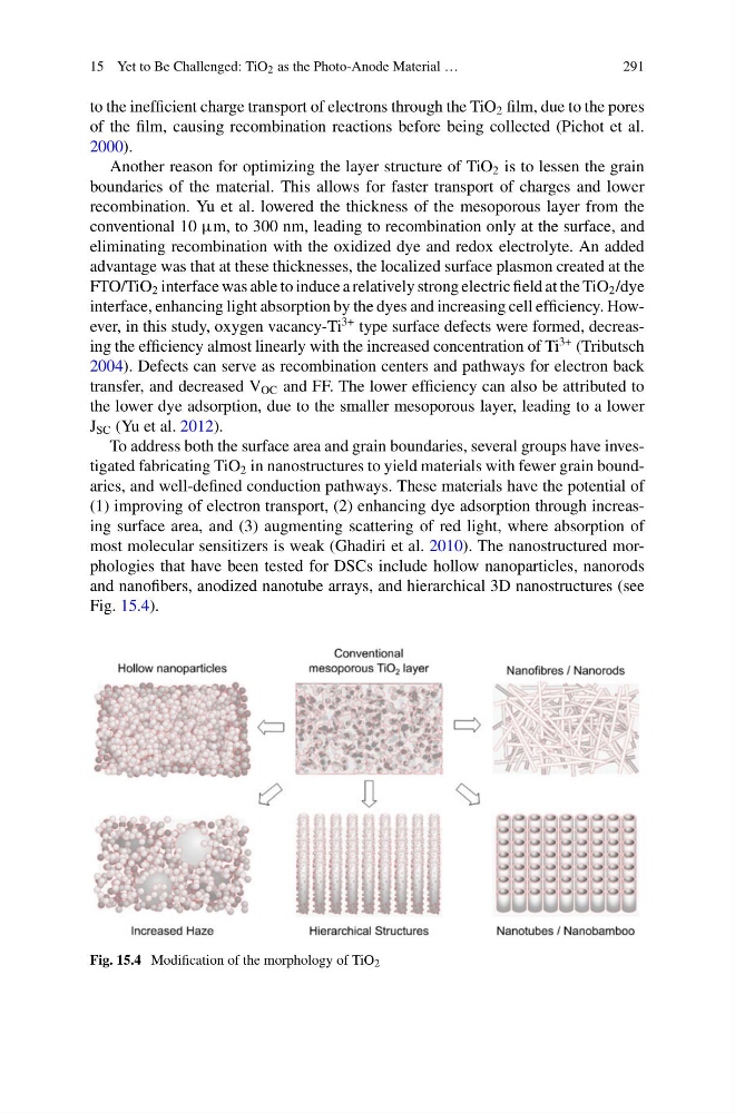
most molecular sensitizers is weak (Ghadiri et al. 2010). The nanostructured morphologies that have been tested for DSCs include hollow nanoparticles, nanorods
and nanofibers, anodized nanotube arrays, and hierarchical 3D nanostructures (see
Fig. 15.4).
Fig. 15.4 Modification of the morphology of TiO 2
291
to the inefficient charge transport of electrons through the TiO 2 film, due to the pores
of the film, causing recombination reactions before being collected (Pichot et al.
2000).
Another reason for optimizing the layer structure of TiO 2 is to lessen the grain
boundaries of the material. This allows for faster transport of charges and lower
recombination. Yu et al. lowered the thickness of the mesoporous layer from the
conventional 10 μm, to 300 nm, leading to recombination only at the surface, and
eliminating recombination with the oxidized dye and redox electrolyte. An added
advantage was that at these thicknesses, the localized surface plasmon created at the
FTO/TiO 2 interface was able to induce a relatively strong electric field at the TiO 2 /dye
interface, enhancing light absorption by the dyes and increasing cell efficiency. However, in this study, oxygen vacancy-Ti
3+ type surface defects were formed, decreasing the efficiency almost linearly with the increased concentration of Ti
3+ (Tributsch
2004). Defects can serve as recombination centers and pathways for electron back
transfer, and decreased V OC and FF. The lower efficiency can also be attributed to
the lower dye adsorption, due to the smaller mesoporous layer, leading to a lower
J SC (Yu et al. 2012).
To address both the surface area and grain boundaries, several groups have investigated fabricating TiO 2 in nanostructures to yield materials with fewer grain boundaries, and well-defined conduction pathways. These materials have the potential of
(1) improving of electron transport, (2) enhancing dye adsorption through increasing surface area, and (3) augmenting scattering of red light, where absorption of
most molecular sensitizers is weak (Ghadiri et al. 2010). The nanostructured morphologies that have been tested for DSCs include hollow nanoparticles, nanorods
and nanofibers, anodized nanotube arrays, and hierarchical 3D nanostructures (see
Fig. 15.4).
Fig. 15.4 Modification of the morphology of TiO 2