

1 Introduction
11
a)
b)
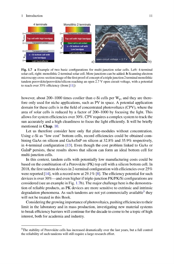
Fig. 1.7 a Example of two basic configurations for multi-junction solar cells. Left: 4-terminal
solar cell, right: monolithic 2-terminal solar cell. More junctions can be added; b Scanning electron
microscopy cross-section image of the first proof of concept of a triple junction 2 terminal monolithic
tandem perovskite/perovskite/silicon reaching an open 2.7 V open circuit voltage, with a potential
to reach over 35% efficiency (from [11])
however, about 200–1000 times costlier than c-Si cells per W p , and they are therefore only used for niche applications, such as PV in space. A potential application
domain for these cells is in the field of concentrated photovoltaics (CPV), where the
area of solar cells is reduced by a factor of 200–1000 by focusing the light. This
allows for system efficiencies over 30%. CPV requires a complex system to track the
sun accurately and a high cleanliness to focus the light efficiently. It will be briefly
mentioned in Chap. 10.
Let us therefore consider here only flat plate-modules without concentration.
Using c-Si as “low cost” bottom cells, record efficiencies could be obtained combining GaAs on silicon and GaAs/InP on silicon at 32.8% and 35.9% respectively,
in 4-terminal configuration [13]. Even though the cost problem linked to GaAs or
GaInP persists, these results shows that silicon can form an ideal bottom cell for
multi-junction cells.
In this context, tandem cells with potentially low manufacturing costs could be
based on the combination of a Perovskite (PK) top cell with a silicon bottom cell. In
2018, the first tandem devices in 2-terminal configuration with efficiencies over 25%
were reported [14], with a record now at 29.1% [8]. The efficiency potential for such
devices is over 30%—and even higher if triple-junction PK/PK/Si configurations are
considered (see an example in Fig. 1.7b). The major challenge here is the demonstration of reliable products, as PK devices are more sensitive to extrinsic and intrinsic
degradation phenomena. As such tandems are not yet commercially available
5 they
will not be treated in this Book.
Considering the growing importance of photovoltaics, pushing efficiencies to their
limit in the laboratory and in mass production, investigating new material systems
to break efficiency barriers will continue for the decade to come to be a topic of high
interest, both for academia and industry.
5 The stability of Perovskite cells has increased dramatically over the last years, but a full control
the reliability of such tandems will still require a large research effort.
11
a)
b)
Fig. 1.7 a Example of two basic configurations for multi-junction solar cells. Left: 4-terminal
solar cell, right: monolithic 2-terminal solar cell. More junctions can be added; b Scanning electron
microscopy cross-section image of the first proof of concept of a triple junction 2 terminal monolithic
tandem perovskite/perovskite/silicon reaching an open 2.7 V open circuit voltage, with a potential
to reach over 35% efficiency (from [11])
however, about 200–1000 times costlier than c-Si cells per W p , and they are therefore only used for niche applications, such as PV in space. A potential application
domain for these cells is in the field of concentrated photovoltaics (CPV), where the
area of solar cells is reduced by a factor of 200–1000 by focusing the light. This
allows for system efficiencies over 30%. CPV requires a complex system to track the
sun accurately and a high cleanliness to focus the light efficiently. It will be briefly
mentioned in Chap. 10.
Let us therefore consider here only flat plate-modules without concentration.
Using c-Si as “low cost” bottom cells, record efficiencies could be obtained combining GaAs on silicon and GaAs/InP on silicon at 32.8% and 35.9% respectively,
in 4-terminal configuration [13]. Even though the cost problem linked to GaAs or
GaInP persists, these results shows that silicon can form an ideal bottom cell for
multi-junction cells.
In this context, tandem cells with potentially low manufacturing costs could be
based on the combination of a Perovskite (PK) top cell with a silicon bottom cell. In
2018, the first tandem devices in 2-terminal configuration with efficiencies over 25%
were reported [14], with a record now at 29.1% [8]. The efficiency potential for such
devices is over 30%—and even higher if triple-junction PK/PK/Si configurations are
considered (see an example in Fig. 1.7b). The major challenge here is the demonstration of reliable products, as PK devices are more sensitive to extrinsic and intrinsic
degradation phenomena. As such tandems are not yet commercially available
5 they
will not be treated in this Book.
Considering the growing importance of photovoltaics, pushing efficiencies to their
limit in the laboratory and in mass production, investigating new material systems
to break efficiency barriers will continue for the decade to come to be a topic of high
interest, both for academia and industry.
5 The stability of Perovskite cells has increased dramatically over the last years, but a full control
the reliability of such tandems will still require a large research effort.