

8 CdTe and CuInGaSe 2 Thin-Film Solar Cells
205
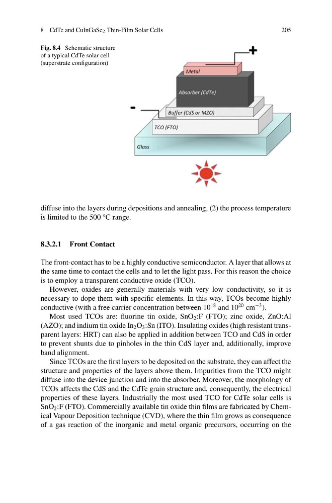
Fig. 8.4 Schematic structure
of a typical CdTe solar cell
(superstrate configuration)
diffuse into the layers during depositions and annealing, (2) the process temperature
is limited to the 500 °C range.
8.3.2.1 Front Contact
The front-contact has to be a highly conductive semiconductor. A layer that allows at
the same time to contact the cells and to let the light pass. For this reason the choice
is to employ a transparent conductive oxide (TCO).
However, oxides are generally materials with very low conductivity, so it is
necessary to dope them with specific elements. In this way, TCOs become highly
conductive (with a free carrier concentration between 10
18 and 10
20 cm
−3 ).
Most used TCOs are: fluorine tin oxide, SnO 2 :F (FTO); zinc oxide, ZnO:Al
(AZO); and indium tin oxide In 2 O 3 :Sn (ITO). Insulating oxides (high resistant transparent layers: HRT) can also be applied in addition between TCO and CdS in order
to prevent shunts due to pinholes in the thin CdS layer and, additionally, improve
band alignment.
Since TCOs are the first layers to be deposited on the substrate, they can affect the
structure and properties of the layers above them. Impurities from the TCO might
diffuse into the device junction and into the absorber. Moreover, the morphology of
TCOs affects the CdS and the CdTe grain structure and, consequently, the electrical
properties of these layers. Industrially the most used TCO for CdTe solar cells is
SnO 2 :F (FTO). Commercially available tin oxide thin films are fabricated by Chemical Vapour Deposition technique (CVD), where the thin film grows as consequence
of a gas reaction of the inorganic and metal organic precursors, occurring on the
205
Fig. 8.4 Schematic structure
of a typical CdTe solar cell
(superstrate configuration)
diffuse into the layers during depositions and annealing, (2) the process temperature
is limited to the 500 °C range.
8.3.2.1 Front Contact
The front-contact has to be a highly conductive semiconductor. A layer that allows at
the same time to contact the cells and to let the light pass. For this reason the choice
is to employ a transparent conductive oxide (TCO).
However, oxides are generally materials with very low conductivity, so it is
necessary to dope them with specific elements. In this way, TCOs become highly
conductive (with a free carrier concentration between 10
18 and 10
20 cm
−3 ).
Most used TCOs are: fluorine tin oxide, SnO 2 :F (FTO); zinc oxide, ZnO:Al
(AZO); and indium tin oxide In 2 O 3 :Sn (ITO). Insulating oxides (high resistant transparent layers: HRT) can also be applied in addition between TCO and CdS in order
to prevent shunts due to pinholes in the thin CdS layer and, additionally, improve
band alignment.
Since TCOs are the first layers to be deposited on the substrate, they can affect the
structure and properties of the layers above them. Impurities from the TCO might
diffuse into the device junction and into the absorber. Moreover, the morphology of
TCOs affects the CdS and the CdTe grain structure and, consequently, the electrical
properties of these layers. Industrially the most used TCO for CdTe solar cells is
SnO 2 :F (FTO). Commercially available tin oxide thin films are fabricated by Chemical Vapour Deposition technique (CVD), where the thin film grows as consequence
of a gas reaction of the inorganic and metal organic precursors, occurring on the