

176
S. Leu and D. Sontag
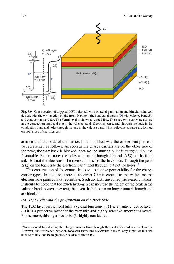
Fig. 7.9 Cross-section of a typical HJT solar cell with bilateral passivation and bifacial solar cell
design, with the p-n junction on the front. Next to it the bandgap diagram [9] with valence band E V
and conduction band E C . The Fermi level is shown as dotted line. There are two narrow peaks one
in the conduction band and one in the valence band. Electrons can tunnel through the peak in the
conduction band and holes through the one in the valence band. Thus, selective contacts are formed
on both sides of the solar cell
area on the other side of the barrier. In a simplified way the carrier transport can
be represented as follows: As soon as the charge carriers are on the other side of
the peak, the way back is blocked, because the starting point is energetically less
favourable. Furthermore: the holes can tunnel through the peak E
V on the front
side, but not the electrons. The reverse is true on the back side. Through the peak
E
C on the back side the electrons can tunnel through, but not the holes.
14
This construction of the contact leads to a selective permeability for the charge
carrier types. In addition, there is no direct Ohmic contact to the wafer and the
electron-hole pairs cannot recombine. Such contacts are called passivated contacts.
It should be noted that too much hydrogen can increase the height of the peak in the
valence band to such an extent, that even the holes can no longer tunnel through and
are blocked.
(b) HJT Cells with the pn-Junction on the Back Side
The TCO layer on the front fulfills several functions: (1) It is an anti-reflective layer,
(2) it is a protective layer for the very thin and highly sensitive amorphous layers.
Furthermore, this layer has to be (3) highly conductive.
14 In a more detailed view, the charge carriers flow through the peaks forward and backwards.
However, the difference between forwards rates and backwards rates is very large, so that the
backward flow can be neglected. See also footnote 10.
S. Leu and D. Sontag
Fig. 7.9 Cross-section of a typical HJT solar cell with bilateral passivation and bifacial solar cell
design, with the p-n junction on the front. Next to it the bandgap diagram [9] with valence band E V
and conduction band E C . The Fermi level is shown as dotted line. There are two narrow peaks one
in the conduction band and one in the valence band. Electrons can tunnel through the peak in the
conduction band and holes through the one in the valence band. Thus, selective contacts are formed
on both sides of the solar cell
area on the other side of the barrier. In a simplified way the carrier transport can
be represented as follows: As soon as the charge carriers are on the other side of
the peak, the way back is blocked, because the starting point is energetically less
favourable. Furthermore: the holes can tunnel through the peak E
V on the front
side, but not the electrons. The reverse is true on the back side. Through the peak
E
C on the back side the electrons can tunnel through, but not the holes.
14
This construction of the contact leads to a selective permeability for the charge
carrier types. In addition, there is no direct Ohmic contact to the wafer and the
electron-hole pairs cannot recombine. Such contacts are called passivated contacts.
It should be noted that too much hydrogen can increase the height of the peak in the
valence band to such an extent, that even the holes can no longer tunnel through and
are blocked.
(b) HJT Cells with the pn-Junction on the Back Side
The TCO layer on the front fulfills several functions: (1) It is an anti-reflective layer,
(2) it is a protective layer for the very thin and highly sensitive amorphous layers.
Furthermore, this layer has to be (3) highly conductive.
14 In a more detailed view, the charge carriers flow through the peaks forward and backwards.
However, the difference between forwards rates and backwards rates is very large, so that the
backward flow can be neglected. See also footnote 10.