

7 Crystalline Silicon Solar Cells: Heterojunction Cells
169
7.2.2 The Basic Structure of a Heterojunction Cell
(a) Two Different Semiconductors
Heterojunction technology uses two materials with different energy bandgaps.
«Hetero»
4 means “different” in Greek. This is the big difference with the so-called
“homo
5 -junction cells” discussed in Chap. 5 (PERC cells). In the case of the heterojunction silicon solar cell, the following two materials are used: crystalline silicon
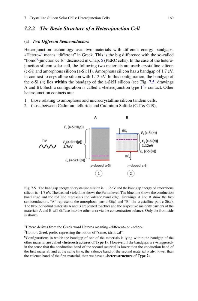
(c-Si) and amorphous silicon (a-Si: H). Amorphous silicon has a bandgap of 1.7 eV,
in contrast to crystalline silicon with 1.12 eV. In this configuration, the bandgap of
the c-Si (n) lies within the bandgap of the a-Si:H silicon (see Fig. 7.5. drawings
A and B). Such a configuration is called a «heterojunction type 1
6 » contact. Other
heterojunction contacts are:
1. those relating to amorphous and microcrystalline silicon tandem cells,
2. those between Cadmium telluride and Cadmium Sulfide (CdTe/ CdS),
Fig. 7.5 The bandgap energy of crystalline silicon is 1.12 eV and the bandgap energy of amorphous
silicon is ~1.7 eV. The dashed violet line shows the Fermi level. The blue line shows the conduction
band edge and the red line represents the valence band edge. Drawings A and B show the two
semiconductors. “A” represents the amorphous part a-Si(p) and “B” the crystalline part c-Si(n).
The two individual materials A and B are joined together and the respective majority carriers of the
materials A and B will diffuse into the other area via the concentration balance. Only the front side
is shown
4 Hetero derives from the Greek word Heteros meaning «different» or «other».
5 Homo-, Greek prefix expressing the notion of “same, identical”.
6 Configurations in which the bandgap of one of the materials is lying within the bandgap of the
other material are called «heterostructures of Type 1». However, if the bandgaps are «staggered»
in the sense that the conduction band of the second material is lower than the conduction band of
the first material, and at the same time, the valence band of the second material is also lower than
the valence band of the first material, then we have a «heterostructure of Type 2».
169
7.2.2 The Basic Structure of a Heterojunction Cell
(a) Two Different Semiconductors
Heterojunction technology uses two materials with different energy bandgaps.
«Hetero»
4 means “different” in Greek. This is the big difference with the so-called
“homo
5 -junction cells” discussed in Chap. 5 (PERC cells). In the case of the heterojunction silicon solar cell, the following two materials are used: crystalline silicon
(c-Si) and amorphous silicon (a-Si: H). Amorphous silicon has a bandgap of 1.7 eV,
in contrast to crystalline silicon with 1.12 eV. In this configuration, the bandgap of
the c-Si (n) lies within the bandgap of the a-Si:H silicon (see Fig. 7.5. drawings
A and B). Such a configuration is called a «heterojunction type 1
6 » contact. Other
heterojunction contacts are:
1. those relating to amorphous and microcrystalline silicon tandem cells,
2. those between Cadmium telluride and Cadmium Sulfide (CdTe/ CdS),
Fig. 7.5 The bandgap energy of crystalline silicon is 1.12 eV and the bandgap energy of amorphous
silicon is ~1.7 eV. The dashed violet line shows the Fermi level. The blue line shows the conduction
band edge and the red line represents the valence band edge. Drawings A and B show the two
semiconductors. “A” represents the amorphous part a-Si(p) and “B” the crystalline part c-Si(n).
The two individual materials A and B are joined together and the respective majority carriers of the
materials A and B will diffuse into the other area via the concentration balance. Only the front side
is shown
4 Hetero derives from the Greek word Heteros meaning «different» or «other».
5 Homo-, Greek prefix expressing the notion of “same, identical”.
6 Configurations in which the bandgap of one of the materials is lying within the bandgap of the
other material are called «heterostructures of Type 1». However, if the bandgaps are «staggered»
in the sense that the conduction band of the second material is lower than the conduction band of
the first material, and at the same time, the valence band of the second material is also lower than
the valence band of the first material, then we have a «heterostructure of Type 2».