

6 Amorphous Silicon Solar Cells
145
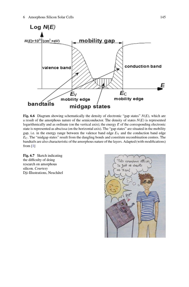
Fig. 6.6 Diagram showing schematically the density of electronic “gap states” N(E), which are
a result of the amorphous nature of the semiconductor. The density of states N(E) is represented
logarithmically and as ordinate (on the vertical axis); the energy E of the corresponding electronic
state is represented as abscissa (on the horizontal axis). The “gap states” are situated in the mobility
gap, i.e. in the energy range between the valence band edge E V and the conduction band edge
E C . The “midgap states” result from the dangling bonds and constitute recombination centres. The
bandtails are also characteristic of the amorphous nature of the layers. Adapted (with modifications)
from [1]
Fig. 6.7 Sketch indicating
the difficulty of doing
research on amorphous
silicon. Courtesy
Dji-Illustrations, Neuchâtel
145
Fig. 6.6 Diagram showing schematically the density of electronic “gap states” N(E), which are
a result of the amorphous nature of the semiconductor. The density of states N(E) is represented
logarithmically and as ordinate (on the vertical axis); the energy E of the corresponding electronic
state is represented as abscissa (on the horizontal axis). The “gap states” are situated in the mobility
gap, i.e. in the energy range between the valence band edge E V and the conduction band edge
E C . The “midgap states” result from the dangling bonds and constitute recombination centres. The
bandtails are also characteristic of the amorphous nature of the layers. Adapted (with modifications)
from [1]
Fig. 6.7 Sketch indicating
the difficulty of doing
research on amorphous
silicon. Courtesy
Dji-Illustrations, Neuchâtel