

5 Crystalline Silicon Solar Cells: Homojunction Cells
111
ingots thin wafers are cut out, which are processed into solar cells. Via a temperaturecontrolled diffusion process,
13 the top side of the wafer is doped with phosphorous.
14 At over 800 °C, one drives this phosphorous about 100–300 nm deep into the
wafer.
15 By doing so, phosphorous atoms sit inside the crystal and occupy the place
where normally a silicon atom should be. This is how the pn-junction is formed in
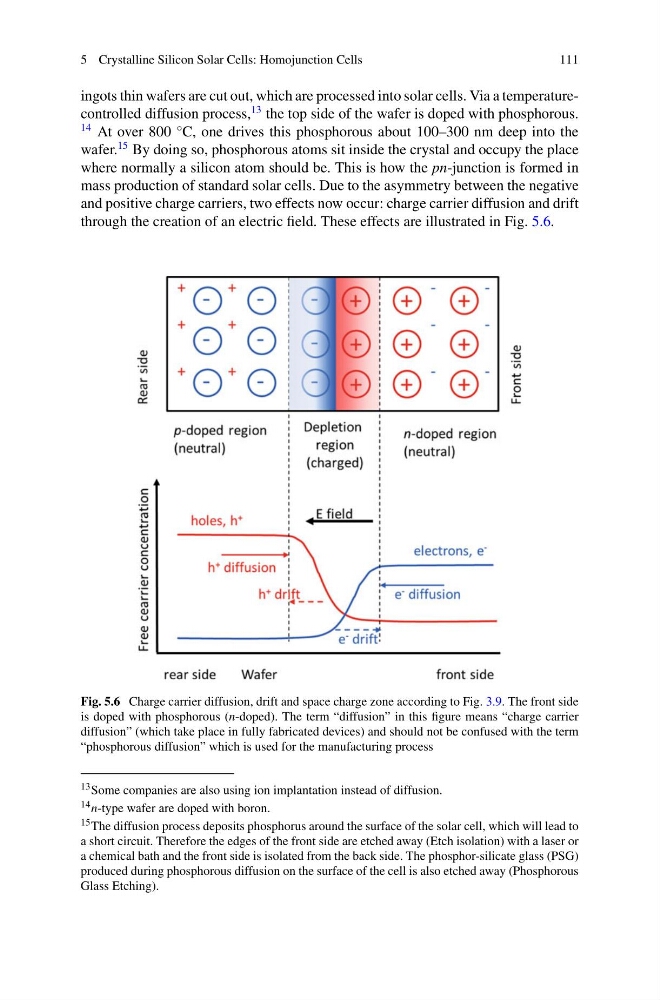
mass production of standard solar cells. Due to the asymmetry between the negative
and positive charge carriers, two effects now occur: charge carrier diffusion and drift
through the creation of an electric field. These effects are illustrated in Fig. 5.6.
Fig. 5.6 Charge carrier diffusion, drift and space charge zone according to Fig. 3.9. The front side
is doped with phosphorous (n-doped). The term “diffusion” in this figure means “charge carrier
diffusion” (which take place in fully fabricated devices) and should not be confused with the term
“phosphorous diffusion” which is used for the manufacturing process
13 Some companies are also using ion implantation instead of diffusion.
14 n-type wafer are doped with boron.
15 The diffusion process deposits phosphorus around the surface of the solar cell, which will lead to
a short circuit. Therefore the edges of the front side are etched away (Etch isolation) with a laser or
a chemical bath and the front side is isolated from the back side. The phosphor-silicate glass (PSG)
produced during phosphorous diffusion on the surface of the cell is also etched away (Phosphorous
Glass Etching).
111
ingots thin wafers are cut out, which are processed into solar cells. Via a temperaturecontrolled diffusion process,
13 the top side of the wafer is doped with phosphorous.
14 At over 800 °C, one drives this phosphorous about 100–300 nm deep into the
wafer.
15 By doing so, phosphorous atoms sit inside the crystal and occupy the place
where normally a silicon atom should be. This is how the pn-junction is formed in
mass production of standard solar cells. Due to the asymmetry between the negative
and positive charge carriers, two effects now occur: charge carrier diffusion and drift
through the creation of an electric field. These effects are illustrated in Fig. 5.6.
Fig. 5.6 Charge carrier diffusion, drift and space charge zone according to Fig. 3.9. The front side
is doped with phosphorous (n-doped). The term “diffusion” in this figure means “charge carrier
diffusion” (which take place in fully fabricated devices) and should not be confused with the term
“phosphorous diffusion” which is used for the manufacturing process
13 Some companies are also using ion implantation instead of diffusion.
14 n-type wafer are doped with boron.
15 The diffusion process deposits phosphorus around the surface of the solar cell, which will lead to
a short circuit. Therefore the edges of the front side are etched away (Etch isolation) with a laser or
a chemical bath and the front side is isolated from the back side. The phosphor-silicate glass (PSG)
produced during phosphorous diffusion on the surface of the cell is also etched away (Phosphorous
Glass Etching).