

86
S. Leu and D. Sontag
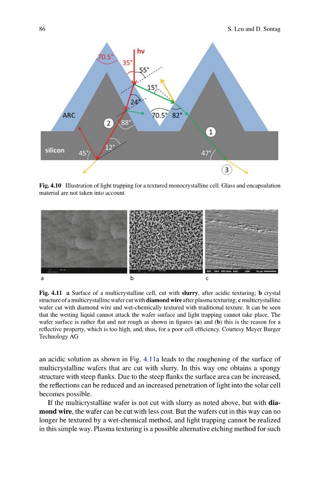
Fig. 4.10 Illustration of light trapping for a textured monocrystalline cell. Glass and encapsulation
material are not taken into account
a
b
c
Fig. 4.11 a Surface of a multicrystalline cell, cut with slurry, after acidic texturing; b crystal
structure of a multicrystalline wafer cut with diamond wire after plasma texturing; c multicrystalline
wafer cut with diamond wire and wet-chemically textured with traditional texture. It can be seen
that the wetting liquid cannot attack the wafer surface and light trapping cannot take place. The
wafer surface is rather flat and not rough as shown in figures (a) and (b) this is the reason for a
reflective property, which is too high, and, thus, for a poor cell efficiency. Courtesy Meyer Burger
Technology AG
an acidic solution as shown in Fig. 4.11a leads to the roughening of the surface of
multicrystalline wafers that are cut with slurry. In this way one obtains a spongy
structure with steep flanks. Due to the steep flanks the surface area can be increased,
the reflections can be reduced and an increased penetration of light into the solar cell
becomes possible.
If the multicrystalline wafer is not cut with slurry as noted above, but with diamond wire, the wafer can be cut with less cost. But the wafers cut in this way can no
longer be textured by a wet-chemical method, and light trapping cannot be realized
in this simple way. Plasma texturing is a possible alternative etching method for such
S. Leu and D. Sontag
Fig. 4.10 Illustration of light trapping for a textured monocrystalline cell. Glass and encapsulation
material are not taken into account
a
b
c
Fig. 4.11 a Surface of a multicrystalline cell, cut with slurry, after acidic texturing; b crystal
structure of a multicrystalline wafer cut with diamond wire after plasma texturing; c multicrystalline
wafer cut with diamond wire and wet-chemically textured with traditional texture. It can be seen
that the wetting liquid cannot attack the wafer surface and light trapping cannot take place. The
wafer surface is rather flat and not rough as shown in figures (a) and (b) this is the reason for a
reflective property, which is too high, and, thus, for a poor cell efficiency. Courtesy Meyer Burger
Technology AG
an acidic solution as shown in Fig. 4.11a leads to the roughening of the surface of
multicrystalline wafers that are cut with slurry. In this way one obtains a spongy
structure with steep flanks. Due to the steep flanks the surface area can be increased,
the reflections can be reduced and an increased penetration of light into the solar cell
becomes possible.
If the multicrystalline wafer is not cut with slurry as noted above, but with diamond wire, the wafer can be cut with less cost. But the wafers cut in this way can no
longer be textured by a wet-chemical method, and light trapping cannot be realized
in this simple way. Plasma texturing is a possible alternative etching method for such