

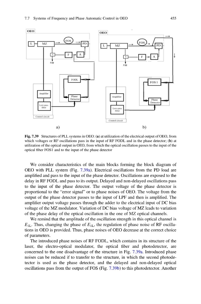
We consider characteristics of the main blocks forming the block diagram of
OEO with PLL system (Fig. 7.39a). Electrical oscillations from the PD load are
amplified and pass to the input of the phase detector. Oscillations are exposed to the
delay in RF FODL and pass to its output. Delayed and non-delayed oscillations pass
to the input of the phase detector. The output voltage of the phase detector is
proportional to the “error signal” or to phase noises of OEO. The voltage from the
output of the phase detector passes to the input of LPF and then is amplified. The
amplifier output voltage passes through the adder to the electrical input of DC bias
voltage of the MZ modulator. Variation of DC bias voltage of MZ leads to variation
of the phase delay of the optical oscillation in the one of MZ optical channels.
We remind that the amplitude of the oscillation strength in this optical channel is
E 1L . Thus, changing the phase of E 1L , the regulation of phase noise of RF oscillations in OEO is provided. Thus, phase noises of OEO decrease at the correct choice
of parameters.
The introduced phase noises of RF FODL, which contains in its structure of the
laser, the electro-optical modulator, the optical fiber and photodetector, are
concerned to the one disadvantage of the structure in Fig. 7.39a. Introduced phase
noises can be reduced if to transfer to the structure, in which the second photodetector is used as the phase detector, and the delayed and non-delayed optical
oscillations pass from the output of FOS (Fig. 7.39b) to this photodetector. Another
Fig. 7.39 Structures of PLL systems in OEO: (a) at utilization of the electrical output of OEO, from
which voltages or RF oscillations pass in the input of RF FODL and in the phase detector; (b) at
utilization of the optical output in OEO, from which the optical oscillation passes to the input of the
optical fiber FOS1 and to the input of the phase detector
7.7 Systems of Frequency and Phase Automatic Control in OEO
455
OEO with PLL system (Fig. 7.39a). Electrical oscillations from the PD load are
amplified and pass to the input of the phase detector. Oscillations are exposed to the
delay in RF FODL and pass to its output. Delayed and non-delayed oscillations pass
to the input of the phase detector. The output voltage of the phase detector is
proportional to the “error signal” or to phase noises of OEO. The voltage from the
output of the phase detector passes to the input of LPF and then is amplified. The
amplifier output voltage passes through the adder to the electrical input of DC bias
voltage of the MZ modulator. Variation of DC bias voltage of MZ leads to variation
of the phase delay of the optical oscillation in the one of MZ optical channels.
We remind that the amplitude of the oscillation strength in this optical channel is
E 1L . Thus, changing the phase of E 1L , the regulation of phase noise of RF oscillations in OEO is provided. Thus, phase noises of OEO decrease at the correct choice
of parameters.
The introduced phase noises of RF FODL, which contains in its structure of the
laser, the electro-optical modulator, the optical fiber and photodetector, are
concerned to the one disadvantage of the structure in Fig. 7.39a. Introduced phase
noises can be reduced if to transfer to the structure, in which the second photodetector is used as the phase detector, and the delayed and non-delayed optical
oscillations pass from the output of FOS (Fig. 7.39b) to this photodetector. Another
Fig. 7.39 Structures of PLL systems in OEO: (a) at utilization of the electrical output of OEO, from
which voltages or RF oscillations pass in the input of RF FODL and in the phase detector; (b) at
utilization of the optical output in OEO, from which the optical oscillation passes to the input of the
optical fiber FOS1 and to the input of the phase detector
7.7 Systems of Frequency and Phase Automatic Control in OEO
455