

density of the phase noise of QWLD output emission, the directional pattern of
output emission can be attributed to the main characteristics of QWLD besides AFC
and PSD.
7.3.3 QWLD Differential Equations and the Transfer
Function
To determine the analytical connection of the QWLD bias current with the OEO
generation frequency, we derive expressions for the QWLD transfer function on the
base of its velocity equations. In [9–12] shows the structural diagram and the QWLD
equivalent circuit without account of the electron–photon resonance. At deriving of
transfer functions, we must take into consideration that usually in order to create the
restrictions of the optical field along the active region, the under-etching to the waveguiding layer thickness of the p-emitter should be 0.1–0.15 μm; the resistance of the
remained layer achieves several hundreds Ω. In this case, we can consider that
capacitances C f and C p-n are connected in series and the charge-discharge of the
capacitance C ¼ C f C p-n /(C f + C p-n ) will be provided through the series-connected
resistances R d and Z d . The value of R d is determined by the resistance of p- and nohmic contacts, by the thickness of the p-emitter over the active region and the
substrate resistance, by the resistance Z d : the parallel-connected capacitance C a and
the impedance of the laser diode Z g . The value of C a is the part of the barrier
capacitance of the p-n junction of the laser’s pumping region. The impedance of
the laser diode is complex, i.e., it consists of the real and reactive parts.
In order to derive the transfer function expressions of the laser diode and its types
of AFC and PFC, we can usually use the various models. We here use the “model
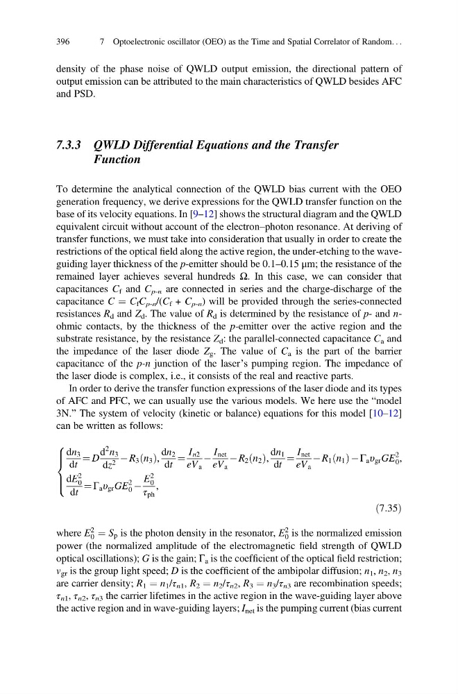
3N.” The system of velocity (kinetic or balance) equations for this model [10–12]
can be written as follows:
dn 3
dt
¼ D
d
2 n 3
dz 2 À R 3 n 3
ð Þ,
dn 2
dt
¼
I n2
eV a
À
I net
eV a
À R 2 n 2
ð Þ,
dn 1
dt
¼
I net
eV a
À R 1 n 1
ð ÞÀΓ a υ gr GE
2
0 ,
dE
2
0
dt
¼ Г a υ gr GE
2
0 À
E
2
0
τ ph
,
8
> > <
> > :
ð7:35Þ
where E
2
0 ¼ S p is the photon density in the resonator, E
2
0 is the normalized emission
power (the normalized amplitude of the electromagnetic field strength of QWLD
optical oscillations); G is the gain; Г а is the coefficient of the optical field restriction;
v gr is the group light speed; D is the coefficient of the ambipolar diffusion; n 1 , n 2 , n 3
are carrier density; R 1 ¼ n 1 /τ n1 , R 2 ¼ n 2 /τ n2 , R 3 ¼ n 3 /τ n3 are recombination speeds;
τ n1 , τ n2 , τ n3 the carrier lifetimes in the active region in the wave-guiding layer above
the active region and in wave-guiding layers; I net is the pumping current (bias current
396
7 Optoelectronic oscillator (OEO) as the Time and Spatial Correlator of Random. . .
output emission can be attributed to the main characteristics of QWLD besides AFC
and PSD.
7.3.3 QWLD Differential Equations and the Transfer
Function
To determine the analytical connection of the QWLD bias current with the OEO
generation frequency, we derive expressions for the QWLD transfer function on the
base of its velocity equations. In [9–12] shows the structural diagram and the QWLD
equivalent circuit without account of the electron–photon resonance. At deriving of
transfer functions, we must take into consideration that usually in order to create the
restrictions of the optical field along the active region, the under-etching to the waveguiding layer thickness of the p-emitter should be 0.1–0.15 μm; the resistance of the
remained layer achieves several hundreds Ω. In this case, we can consider that
capacitances C f and C p-n are connected in series and the charge-discharge of the
capacitance C ¼ C f C p-n /(C f + C p-n ) will be provided through the series-connected
resistances R d and Z d . The value of R d is determined by the resistance of p- and nohmic contacts, by the thickness of the p-emitter over the active region and the
substrate resistance, by the resistance Z d : the parallel-connected capacitance C a and
the impedance of the laser diode Z g . The value of C a is the part of the barrier
capacitance of the p-n junction of the laser’s pumping region. The impedance of
the laser diode is complex, i.e., it consists of the real and reactive parts.
In order to derive the transfer function expressions of the laser diode and its types
of AFC and PFC, we can usually use the various models. We here use the “model
3N.” The system of velocity (kinetic or balance) equations for this model [10–12]
can be written as follows:
dn 3
dt
¼ D
d
2 n 3
dz 2 À R 3 n 3
ð Þ,
dn 2
dt
¼
I n2
eV a
À
I net
eV a
À R 2 n 2
ð Þ,
dn 1
dt
¼
I net
eV a
À R 1 n 1
ð ÞÀΓ a υ gr GE
2
0 ,
dE
2
0
dt
¼ Г a υ gr GE
2
0 À
E
2
0
τ ph
,
8
> > <
> > :
ð7:35Þ
where E
2
0 ¼ S p is the photon density in the resonator, E
2
0 is the normalized emission
power (the normalized amplitude of the electromagnetic field strength of QWLD
optical oscillations); G is the gain; Г а is the coefficient of the optical field restriction;
v gr is the group light speed; D is the coefficient of the ambipolar diffusion; n 1 , n 2 , n 3
are carrier density; R 1 ¼ n 1 /τ n1 , R 2 ¼ n 2 /τ n2 , R 3 ¼ n 3 /τ n3 are recombination speeds;
τ n1 , τ n2 , τ n3 the carrier lifetimes in the active region in the wave-guiding layer above
the active region and in wave-guiding layers; I net is the pumping current (bias current
396
7 Optoelectronic oscillator (OEO) as the Time and Spatial Correlator of Random. . .