

416
22 Layered Structures
the few-layered BP shows high carrier mobility, up to 10
3 cm
2 V
−1 s
−1 , and high
current on/off ratios, up to 10
5 Hz at room temperature. Unrolling the single-walled
carbon nanotubes (SWCNTs) triggers many intriguing properties that cannot be seen
from the CNT or a large graphene sheet [4, 5]. In addition to the observed edge Dirac
fermion states [6, 7] with ultrahigh electrical and thermal conductivity [8], and unexpected magnetization [9, 10], the bandgap of a GNR expands monotonically with
the inverse of ribbon width [5, 11, 12].
One can turn the indirect bandgap of the bulk MoS 2 from 1.2 eV to the direct
bandgap of 1.8 eV by simply reducing the number of layers from infinitely large into
single [13, 14]. The indirect bandgap also degenerates into a direct for the few-layered
MoSe 2 [15]. Bandgap transition from indirect to direct depends not only on the
number of layers but also on the material and the operation conditions [16]. Kelvin and
conductive atomic force microscopy (AFM) revealed that the surface potential well
goes deeper linearly with thickness from the bulk value of −7.2 to −427 mV when the
bulk MoS 2 turns into monolayer [17]. These entities make the 2-D semiconductors an
appealing type of materials for applications as flexible, miniaturized, and wearable
electronic devices and energy management such as photovoltaic cells [18, 19], field
effect transistors [20–22], light-emitting diodes [23, 24], and photodetectors [25–27].
22.2 Orbital Hybridization and Structure Configuration
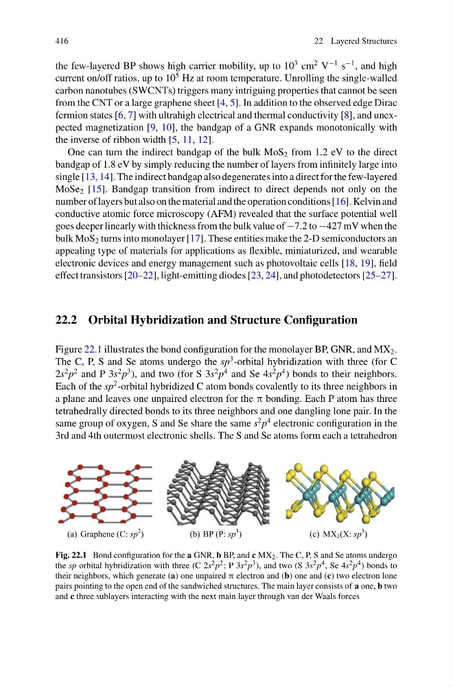
Figure 22.1 illustrates the bond configuration for the monolayer BP, GNR, and MX 2 .
The C, P, S and Se atoms undergo the sp
3 -orbital hybridization with three (for C
2s
2 p
2 and P 3s
2 p
3 ), and two (for S 3s
2 p
4 and Se 4s
2 p
4 ) bonds to their neighbors.
Each of the sp
2 -orbital hybridized C atom bonds covalently to its three neighbors in
a plane and leaves one unpaired electron for the π bonding. Each P atom has three
tetrahedrally directed bonds to its three neighbors and one dangling lone pair. In the
same group of oxygen, S and Se share the same s
2 p
4 electronic configuration in the
3rd and 4th outermost electronic shells. The S and Se atoms form each a tetrahedron
(a) Graphene (C: sp
2
BP (P: sp
3
)
( b )
)
( c )M X 2 (X: sp
3 )
Fig. 22.1 Bond configuration for the a GNR, b BP, and c MX 2 . The C, P, S and Se atoms undergo
the sp orbital hybridization with three (C 2s 2 p 2 ; P 3s 2 p 3 ), and two (S 3s 2 p 4 , Se 4s 2 p 4 ) bonds to
their neighbors, which generate (a) one unpaired π electron and (b) one and (c) two electron lone
pairs pointing to the open end of the sandwiched structures. The main layer consists of a one, b two
and c three sublayers interacting with the next main layer through van der Waals forces
22 Layered Structures
the few-layered BP shows high carrier mobility, up to 10
3 cm
2 V
−1 s
−1 , and high
current on/off ratios, up to 10
5 Hz at room temperature. Unrolling the single-walled
carbon nanotubes (SWCNTs) triggers many intriguing properties that cannot be seen
from the CNT or a large graphene sheet [4, 5]. In addition to the observed edge Dirac
fermion states [6, 7] with ultrahigh electrical and thermal conductivity [8], and unexpected magnetization [9, 10], the bandgap of a GNR expands monotonically with
the inverse of ribbon width [5, 11, 12].
One can turn the indirect bandgap of the bulk MoS 2 from 1.2 eV to the direct
bandgap of 1.8 eV by simply reducing the number of layers from infinitely large into
single [13, 14]. The indirect bandgap also degenerates into a direct for the few-layered
MoSe 2 [15]. Bandgap transition from indirect to direct depends not only on the
number of layers but also on the material and the operation conditions [16]. Kelvin and
conductive atomic force microscopy (AFM) revealed that the surface potential well
goes deeper linearly with thickness from the bulk value of −7.2 to −427 mV when the
bulk MoS 2 turns into monolayer [17]. These entities make the 2-D semiconductors an
appealing type of materials for applications as flexible, miniaturized, and wearable
electronic devices and energy management such as photovoltaic cells [18, 19], field
effect transistors [20–22], light-emitting diodes [23, 24], and photodetectors [25–27].
22.2 Orbital Hybridization and Structure Configuration
Figure 22.1 illustrates the bond configuration for the monolayer BP, GNR, and MX 2 .
The C, P, S and Se atoms undergo the sp
3 -orbital hybridization with three (for C
2s
2 p
2 and P 3s
2 p
3 ), and two (for S 3s
2 p
4 and Se 4s
2 p
4 ) bonds to their neighbors.
Each of the sp
2 -orbital hybridized C atom bonds covalently to its three neighbors in
a plane and leaves one unpaired electron for the π bonding. Each P atom has three
tetrahedrally directed bonds to its three neighbors and one dangling lone pair. In the
same group of oxygen, S and Se share the same s
2 p
4 electronic configuration in the
3rd and 4th outermost electronic shells. The S and Se atoms form each a tetrahedron
(a) Graphene (C: sp
2
BP (P: sp
3
)
( b )
)
( c )M X 2 (X: sp
3 )
Fig. 22.1 Bond configuration for the a GNR, b BP, and c MX 2 . The C, P, S and Se atoms undergo
the sp orbital hybridization with three (C 2s 2 p 2 ; P 3s 2 p 3 ), and two (S 3s 2 p 4 , Se 4s 2 p 4 ) bonds to
their neighbors, which generate (a) one unpaired π electron and (b) one and (c) two electron lone
pairs pointing to the open end of the sandwiched structures. The main layer consists of a one, b two
and c three sublayers interacting with the next main layer through van der Waals forces