

15.3 Cu 3 O 2 Model Reality
311
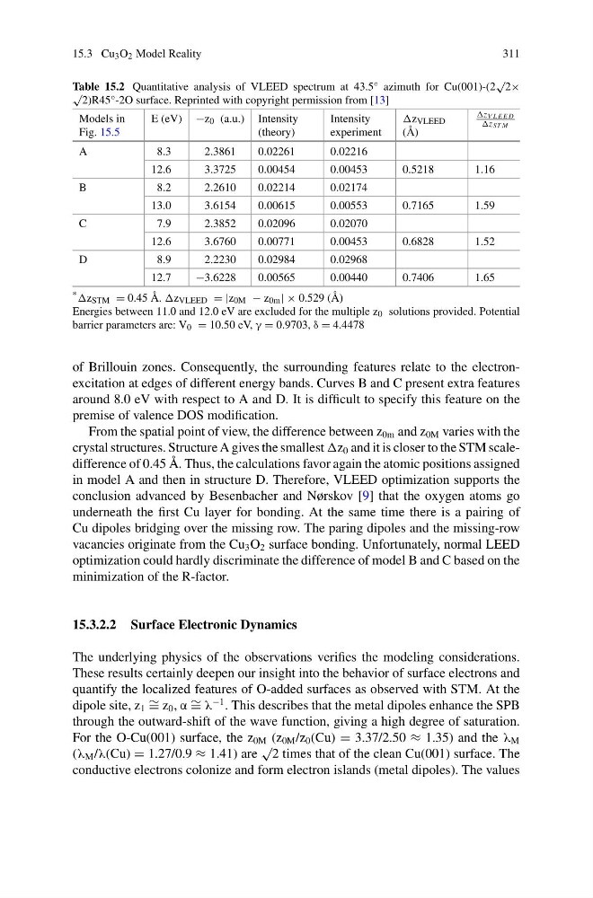
Table 15.2 Quantitative analysis of VLEED spectrum at 43.5° azimuth for Cu(001)-(2
√
2×
√
2)R45°-2O surface. Reprinted with copyright permission from [13]
Models in
Fig. 15.5
E (eV) −z 0 (a.u.) Intensity
(theory)
Intensity
experiment
z VLEED
(Å)
z V L E E D
z ST M
A
8.3
2.3861
0.02261
0.02216
12.6
3.3725
0.00454
0.00453
0.5218
1.16
B
8.2
2.2610
0.02214
0.02174
13.0
3.6154
0.00615
0.00553
0.7165
1.59
C
7.9
2.3852
0.02096
0.02070
12.6
3.6760
0.00771
0.00453
0.6828
1.52
D
8.9
2.2230
0.02984
0.02968
12.7
−3.6228
0.00565
0.00440
0.7406
1.65
* z STM = 0.45 Å. z VLEED = |z 0M − z 0m | × 0.529 (Å)
Energies between 11.0 and 12.0 eV are excluded for the multiple z 0 solutions provided. Potential
barrier parameters are: V 0 = 10.50 eV, γ = 0.9703, δ = 4.4478
of Brillouin zones. Consequently, the surrounding features relate to the electronexcitation at edges of different energy bands. Curves B and C present extra features
around 8.0 eV with respect to A and D. It is difficult to specify this feature on the
premise of valence DOS modification.
From the spatial point of view, the difference between z 0m and z 0M varies with the
crystal structures. Structure A gives the smallest z 0 and it is closer to the STM scaledifference of 0.45 Å. Thus, the calculations favor again the atomic positions assigned
in model A and then in structure D. Therefore, VLEED optimization supports the
conclusion advanced by Besenbacher and Nørskov [9] that the oxygen atoms go
underneath the first Cu layer for bonding. At the same time there is a pairing of
Cu dipoles bridging over the missing row. The paring dipoles and the missing-row
vacancies originate from the Cu 3 O 2 surface bonding. Unfortunately, normal LEED
optimization could hardly discriminate the difference of model B and C based on the
minimization of the R-factor.
15.3.2.2 Surface Electronic Dynamics
The underlying physics of the observations verifies the modeling considerations.
These results certainly deepen our insight into the behavior of surface electrons and
quantify the localized features of O-added surfaces as observed with STM. At the
dipole site, z 1 ∼ = z 0 , α ∼ = λ
−1 . This describes that the metal dipoles enhance the SPB
through the outward-shift of the wave function, giving a high degree of saturation.
For the O-Cu(001) surface, the z 0M (z 0M /z 0 (Cu) = 3.37/2.50 ≈ 1.35) and the λ M
(λ M /λ(Cu) = 1.27/0.9 ≈ 1.41) are
√
2 times that of the clean Cu(001) surface. The
conductive electrons colonize and form electron islands (metal dipoles). The values
311
Table 15.2 Quantitative analysis of VLEED spectrum at 43.5° azimuth for Cu(001)-(2
√
2×
√
2)R45°-2O surface. Reprinted with copyright permission from [13]
Models in
Fig. 15.5
E (eV) −z 0 (a.u.) Intensity
(theory)
Intensity
experiment
z VLEED
(Å)
z V L E E D
z ST M
A
8.3
2.3861
0.02261
0.02216
12.6
3.3725
0.00454
0.00453
0.5218
1.16
B
8.2
2.2610
0.02214
0.02174
13.0
3.6154
0.00615
0.00553
0.7165
1.59
C
7.9
2.3852
0.02096
0.02070
12.6
3.6760
0.00771
0.00453
0.6828
1.52
D
8.9
2.2230
0.02984
0.02968
12.7
−3.6228
0.00565
0.00440
0.7406
1.65
* z STM = 0.45 Å. z VLEED = |z 0M − z 0m | × 0.529 (Å)
Energies between 11.0 and 12.0 eV are excluded for the multiple z 0 solutions provided. Potential
barrier parameters are: V 0 = 10.50 eV, γ = 0.9703, δ = 4.4478
of Brillouin zones. Consequently, the surrounding features relate to the electronexcitation at edges of different energy bands. Curves B and C present extra features
around 8.0 eV with respect to A and D. It is difficult to specify this feature on the
premise of valence DOS modification.
From the spatial point of view, the difference between z 0m and z 0M varies with the
crystal structures. Structure A gives the smallest z 0 and it is closer to the STM scaledifference of 0.45 Å. Thus, the calculations favor again the atomic positions assigned
in model A and then in structure D. Therefore, VLEED optimization supports the
conclusion advanced by Besenbacher and Nørskov [9] that the oxygen atoms go
underneath the first Cu layer for bonding. At the same time there is a pairing of
Cu dipoles bridging over the missing row. The paring dipoles and the missing-row
vacancies originate from the Cu 3 O 2 surface bonding. Unfortunately, normal LEED
optimization could hardly discriminate the difference of model B and C based on the
minimization of the R-factor.
15.3.2.2 Surface Electronic Dynamics
The underlying physics of the observations verifies the modeling considerations.
These results certainly deepen our insight into the behavior of surface electrons and
quantify the localized features of O-added surfaces as observed with STM. At the
dipole site, z 1 ∼ = z 0 , α ∼ = λ
−1 . This describes that the metal dipoles enhance the SPB
through the outward-shift of the wave function, giving a high degree of saturation.
For the O-Cu(001) surface, the z 0M (z 0M /z 0 (Cu) = 3.37/2.50 ≈ 1.35) and the λ M
(λ M /λ(Cu) = 1.27/0.9 ≈ 1.41) are
√
2 times that of the clean Cu(001) surface. The
conductive electrons colonize and form electron islands (metal dipoles). The values