

158
G. Lutz and R. Klanner
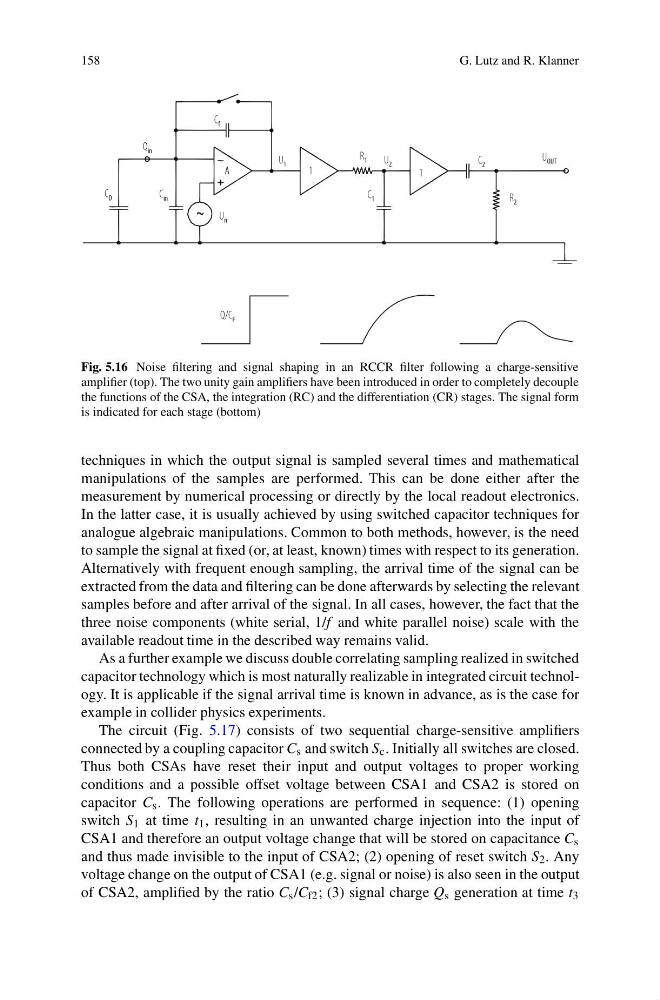
Fig. 5.16 Noise filtering and signal shaping in an RCCR filter following a charge-sensitive
amplifier (top). The two unity gain amplifiers have been introduced in order to completely decouple
the functions of the CSA, the integration (RC) and the differentiation (CR) stages. The signal form
is indicated for each stage (bottom)
techniques in which the output signal is sampled several times and mathematical
manipulations of the samples are performed. This can be done either after the
measurement by numerical processing or directly by the local readout electronics.
In the latter case, it is usually achieved by using switched capacitor techniques for
analogue algebraic manipulations. Common to both methods, however, is the need
to sample the signal at fixed (or, at least, known) times with respect to its generation.
Alternatively with frequent enough sampling, the arrival time of the signal can be
extracted from the data and filtering can be done afterwards by selecting the relevant
samples before and after arrival of the signal. In all cases, however, the fact that the
three noise components (white serial, 1/f and white parallel noise) scale with the
available readout time in the described way remains valid.
As a further example we discuss double correlating sampling realized in switched
capacitor technology which is most naturally realizable in integrated circuit technology. It is applicable if the signal arrival time is known in advance, as is the case for
example in collider physics experiments.
The circuit (Fig. 5.17) consists of two sequential charge-sensitive amplifiers
connected by a coupling capacitor C s and switch S c . Initially all switches are closed.
Thus both CSAs have reset their input and output voltages to proper working
conditions and a possible offset voltage between CSA1 and CSA2 is stored on
capacitor C s . The following operations are performed in sequence: (1) opening
switch S 1 at time t 1 , resulting in an unwanted charge injection into the input of
CSA1 and therefore an output voltage change that will be stored on capacitance C s
and thus made invisible to the input of CSA2; (2) opening of reset switch S 2 . Any
voltage change on the output of CSA1 (e.g. signal or noise) is also seen in the output
of CSA2, amplified by the ratio C s /C f2 ; (3) signal charge Q s generation at time t 3
G. Lutz and R. Klanner
Fig. 5.16 Noise filtering and signal shaping in an RCCR filter following a charge-sensitive
amplifier (top). The two unity gain amplifiers have been introduced in order to completely decouple
the functions of the CSA, the integration (RC) and the differentiation (CR) stages. The signal form
is indicated for each stage (bottom)
techniques in which the output signal is sampled several times and mathematical
manipulations of the samples are performed. This can be done either after the
measurement by numerical processing or directly by the local readout electronics.
In the latter case, it is usually achieved by using switched capacitor techniques for
analogue algebraic manipulations. Common to both methods, however, is the need
to sample the signal at fixed (or, at least, known) times with respect to its generation.
Alternatively with frequent enough sampling, the arrival time of the signal can be
extracted from the data and filtering can be done afterwards by selecting the relevant
samples before and after arrival of the signal. In all cases, however, the fact that the
three noise components (white serial, 1/f and white parallel noise) scale with the
available readout time in the described way remains valid.
As a further example we discuss double correlating sampling realized in switched
capacitor technology which is most naturally realizable in integrated circuit technology. It is applicable if the signal arrival time is known in advance, as is the case for
example in collider physics experiments.
The circuit (Fig. 5.17) consists of two sequential charge-sensitive amplifiers
connected by a coupling capacitor C s and switch S c . Initially all switches are closed.
Thus both CSAs have reset their input and output voltages to proper working
conditions and a possible offset voltage between CSA1 and CSA2 is stored on
capacitor C s . The following operations are performed in sequence: (1) opening
switch S 1 at time t 1 , resulting in an unwanted charge injection into the input of
CSA1 and therefore an output voltage change that will be stored on capacitance C s
and thus made invisible to the input of CSA2; (2) opening of reset switch S 2 . Any
voltage change on the output of CSA1 (e.g. signal or noise) is also seen in the output
of CSA2, amplified by the ratio C s /C f2 ; (3) signal charge Q s generation at time t 3