

ZnSe/ZnS (Ke et al. 2012), ZnS (Koneswaran and Narayanaswamy 2009), CdTe/
CdS (Gui et al. 2012) are some QDs used for sensor applications. These can be
employed for efficient sensing of multiple analytes.
5.3.2.8 Porous Silica
Porous silicon consists of silicon threads with thickness in nanorange (2–5 nm),
arranged in the form of a complicated network, with surface having tiny pores
ranging from nano- to micrometre dimensions. Due to these small pores, this
material is capable of light absorption and emission. This material is semiconductor
in nature with very high internal surface area/volume ratio. The light is emitted in
visible region due to phenomenon of quantum confinement, and the material’s
porosity controls the wavelength of the light emitted. Longer wavelengths are
emitted by less porous silica, while shorter wavelengths are emitted by highly porous
silica. For e.g., silica with porosity >70% emit blue/green light, and porosity ~40%
emit red light. There is also variation in luminescence of porous silica by
incorporation of molecules into the porous surface, making them suitable for application as gas sensors. Visual colour change can be monitored in the porous silica in
the presence of analyte gas molecules, hence causing efficient detection of these
molecules. The properties of porous silica can be modified to have suitable detection
of particular analyte (Dahman et al. 2017).
5.3.3 On the Basis of Applications
As mentioned above, nanosensors find huge applications in almost all areas of life.
Major threat to our health and environment is possessed by chemical pollutants like
aromatic compounds, microorganisms, heavy metals, pesticides, etc., which are
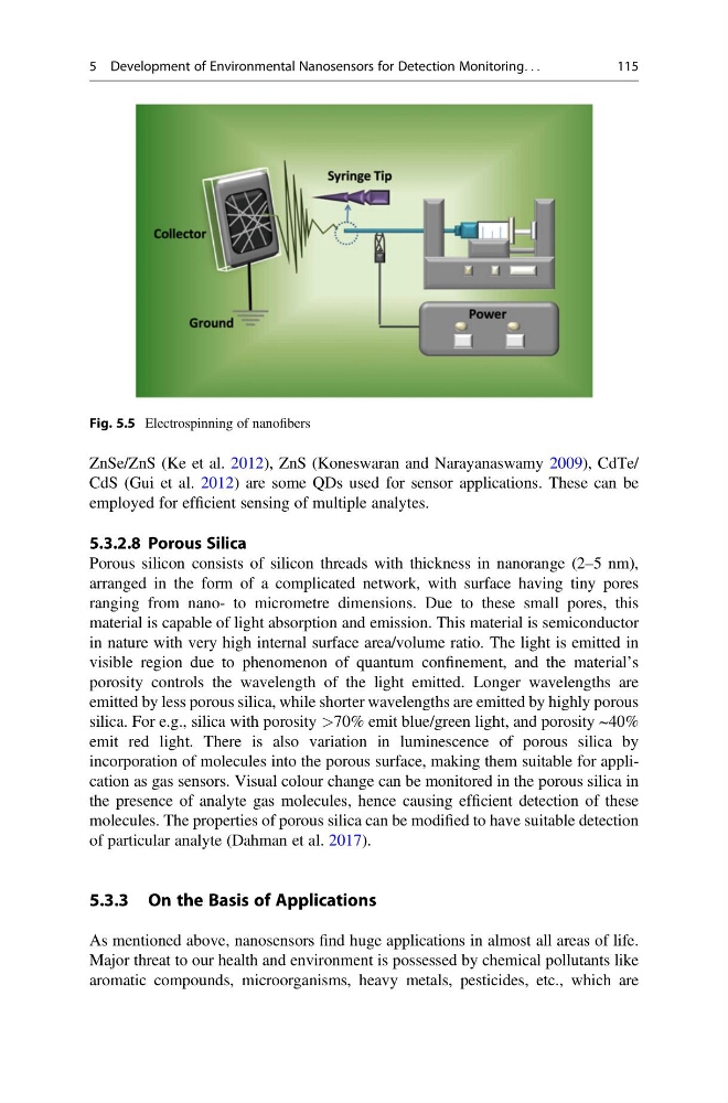
Fig. 5.5 Electrospinning of nanofibers
5 Development of Environmental Nanosensors for Detection Monitoring. . .
115
CdS (Gui et al. 2012) are some QDs used for sensor applications. These can be
employed for efficient sensing of multiple analytes.
5.3.2.8 Porous Silica
Porous silicon consists of silicon threads with thickness in nanorange (2–5 nm),
arranged in the form of a complicated network, with surface having tiny pores
ranging from nano- to micrometre dimensions. Due to these small pores, this
material is capable of light absorption and emission. This material is semiconductor
in nature with very high internal surface area/volume ratio. The light is emitted in
visible region due to phenomenon of quantum confinement, and the material’s
porosity controls the wavelength of the light emitted. Longer wavelengths are
emitted by less porous silica, while shorter wavelengths are emitted by highly porous
silica. For e.g., silica with porosity >70% emit blue/green light, and porosity ~40%
emit red light. There is also variation in luminescence of porous silica by
incorporation of molecules into the porous surface, making them suitable for application as gas sensors. Visual colour change can be monitored in the porous silica in
the presence of analyte gas molecules, hence causing efficient detection of these
molecules. The properties of porous silica can be modified to have suitable detection
of particular analyte (Dahman et al. 2017).
5.3.3 On the Basis of Applications
As mentioned above, nanosensors find huge applications in almost all areas of life.
Major threat to our health and environment is possessed by chemical pollutants like
aromatic compounds, microorganisms, heavy metals, pesticides, etc., which are
Fig. 5.5 Electrospinning of nanofibers
5 Development of Environmental Nanosensors for Detection Monitoring. . .
115