

4.3 Changes in Surface Stress during UPD
129
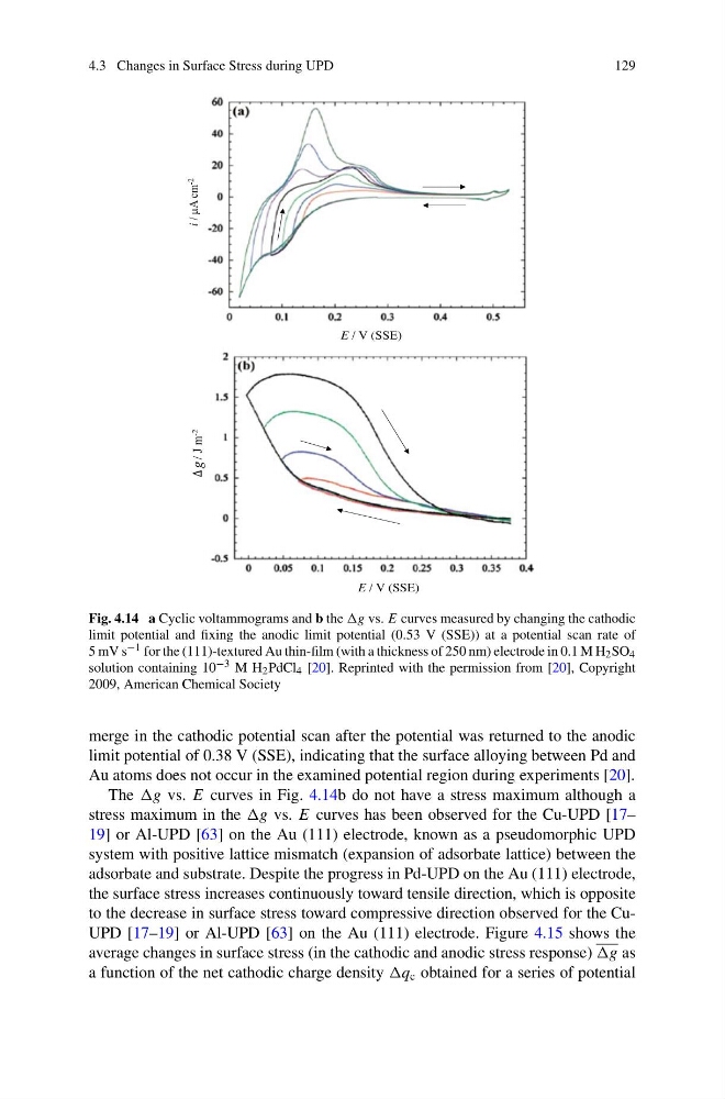
Fig. 4.14 a Cyclic voltammograms and b the vs. E curves measured by changing the cathodic
limit potential and fixing the anodic limit potential (0.53 V (SSE)) at a potential scan rate of
5 mV s −1 for the (111)-textured Au thin-film (with a thickness of 250 nm) electrode in 0.1 M H 2 SO 4
solution containing 10 −3 M H 2 PdCl 4 [20]. Reprinted with the permission from [20], Copyright
2009, American Chemical Society
merge in the cathodic potential scan after the potential was returned to the anodic
limit potential of 0.38 V (SSE), indicating that the surface alloying between Pd and
Au atoms does not occur in the examined potential region during experiments [20].
The vs. E curves in Fig. 4.14b do not have a stress maximum although a
stress maximum in the vs. E curves has been observed for the Cu-UPD [17–
19] or Al-UPD [63] on the Au (111) electrode, known as a pseudomorphic UPD
system with positive lattice mismatch (expansion of adsorbate lattice) between the
adsorbate and substrate. Despite the progress in Pd-UPD on the Au (111) electrode,
the surface stress increases continuously toward tensile direction, which is opposite
to the decrease in surface stress toward compressive direction observed for the CuUPD [17–19] or Al-UPD [63] on the Au (111) electrode. Figure 4.15 shows the
average changes in surface stress (in the cathodic and anodic stress response) as
a function of the net cathodic charge density c obtained for a series of potential
129
Fig. 4.14 a Cyclic voltammograms and b the vs. E curves measured by changing the cathodic
limit potential and fixing the anodic limit potential (0.53 V (SSE)) at a potential scan rate of
5 mV s −1 for the (111)-textured Au thin-film (with a thickness of 250 nm) electrode in 0.1 M H 2 SO 4
solution containing 10 −3 M H 2 PdCl 4 [20]. Reprinted with the permission from [20], Copyright
2009, American Chemical Society
merge in the cathodic potential scan after the potential was returned to the anodic
limit potential of 0.38 V (SSE), indicating that the surface alloying between Pd and
Au atoms does not occur in the examined potential region during experiments [20].
The vs. E curves in Fig. 4.14b do not have a stress maximum although a
stress maximum in the vs. E curves has been observed for the Cu-UPD [17–
19] or Al-UPD [63] on the Au (111) electrode, known as a pseudomorphic UPD
system with positive lattice mismatch (expansion of adsorbate lattice) between the
adsorbate and substrate. Despite the progress in Pd-UPD on the Au (111) electrode,
the surface stress increases continuously toward tensile direction, which is opposite
to the decrease in surface stress toward compressive direction observed for the CuUPD [17–19] or Al-UPD [63] on the Au (111) electrode. Figure 4.15 shows the
average changes in surface stress (in the cathodic and anodic stress response) as
a function of the net cathodic charge density c obtained for a series of potential