

332
R. R. Deshmukh et al.
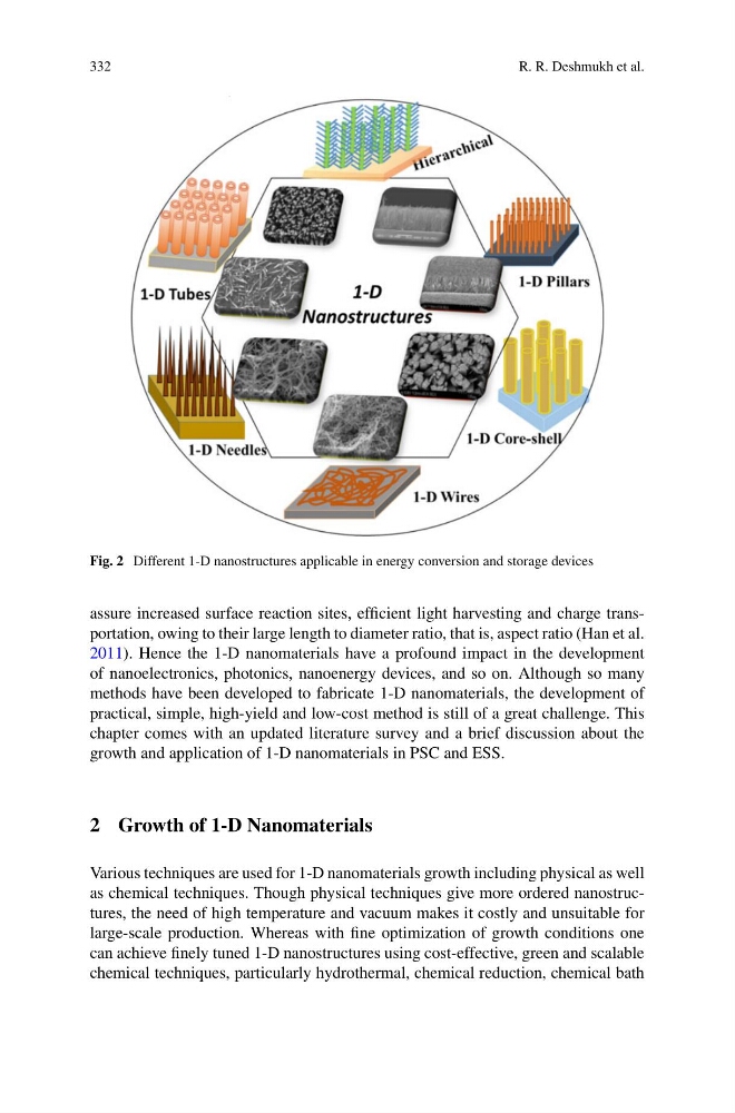
Fig. 2 Different 1-D nanostructures applicable in energy conversion and storage devices
assure increased surface reaction sites, efficient light harvesting and charge transportation, owing to their large length to diameter ratio, that is, aspect ratio (Han et al.
2011). Hence the 1-D nanomaterials have a profound impact in the development
of nanoelectronics, photonics, nanoenergy devices, and so on. Although so many
methods have been developed to fabricate 1-D nanomaterials, the development of
practical, simple, high-yield and low-cost method is still of a great challenge. This
chapter comes with an updated literature survey and a brief discussion about the
growth and application of 1-D nanomaterials in PSC and ESS.
2 Growth of 1-D Nanomaterials
Various techniques are used for 1-D nanomaterials growth including physical as well
as chemical techniques. Though physical techniques give more ordered nanostructures, the need of high temperature and vacuum makes it costly and unsuitable for
large-scale production. Whereas with fine optimization of growth conditions one
can achieve finely tuned 1-D nanostructures using cost-effective, green and scalable
chemical techniques, particularly hydrothermal, chemical reduction, chemical bath
R. R. Deshmukh et al.
Fig. 2 Different 1-D nanostructures applicable in energy conversion and storage devices
assure increased surface reaction sites, efficient light harvesting and charge transportation, owing to their large length to diameter ratio, that is, aspect ratio (Han et al.
2011). Hence the 1-D nanomaterials have a profound impact in the development
of nanoelectronics, photonics, nanoenergy devices, and so on. Although so many
methods have been developed to fabricate 1-D nanomaterials, the development of
practical, simple, high-yield and low-cost method is still of a great challenge. This
chapter comes with an updated literature survey and a brief discussion about the
growth and application of 1-D nanomaterials in PSC and ESS.
2 Growth of 1-D Nanomaterials
Various techniques are used for 1-D nanomaterials growth including physical as well
as chemical techniques. Though physical techniques give more ordered nanostructures, the need of high temperature and vacuum makes it costly and unsuitable for
large-scale production. Whereas with fine optimization of growth conditions one
can achieve finely tuned 1-D nanostructures using cost-effective, green and scalable
chemical techniques, particularly hydrothermal, chemical reduction, chemical bath